

10M08SCE144I7G FPGAs: Features, Applications and Datasheet
2025-03-05 10:27:29 612
10M08SCE144I7G Description
The 10M08SCE144I7G is an Intel MAX® 10 FPGA from the MAX 10 family, designed for applications requiring high performance and efficient integration. It features embedded flash memory, enhanced I/O capabilities, and power-efficient operation, making it ideal for edge computing, signal processing, and control systems.
10M08SCE144I7G Features
Logic Elements (LEs): Up to 8,000 LEs for flexible logic implementation.
Embedded Flash Memory: On-chip flash for configuration storage and user code.
Clock Management: PLLs and internal oscillators for precise clock control.
I/O Support: High-speed differential and single-ended I/Os.
Integrated Analog: ADC blocks for mixed-signal capabilities.
Power Efficiency: Optimized for low-power consumption.
Configuration Modes: Instant-on and multi-configuration support.
10M08SCE144I7G Applications
Industrial automation and motor control systems.
Consumer electronics for high-performance control logic.
Signal processing and digital communications.
Medical instrumentation and portable devices.
IoT edge devices requiring real-time processing.
10M08SCE144I7G CAD Model
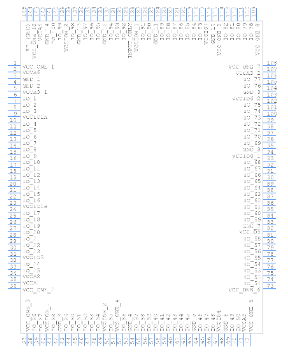
Symbol
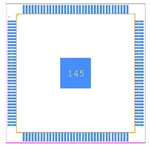
Footprint
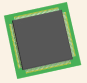
3D Model

10M08SCE144I7G Alternatives
10M04DCF256I7G: A lower-density alternative for applications needing fewer resources.
10M16SCE144I7G: A higher-density alternative for applications needing more logic elements.
Lattice MachXO2-7000HC: For cost-sensitive designs requiring non-volatile FPGA solutions.
Xilinx Spartan-7 XC7S15: Suitable for designs needing advanced logic functionality.
Altera Cyclone IV E EP4CE10F17C8N: Offers competitive logic capacity and power efficiency.
10M08SCE144I7G Manufacturer
Intel Corporation stands as a cornerstone of modern semiconductor innovation, transforming computing since its founding in 1968. Beyond its iconic microprocessors, Intel has evolved into a multifaceted technology leader driving breakthroughs in AI, 5G, and edge computing. Its relentless focus on integrated design and cutting-edge fabrication technologies has enabled the creation of highly efficient, high-performance solutions that power everything from personal devices to massive data centers. What truly distinguishes Intel is its commitment to creating holistic ecosystems that seamlessly connect hardware, software, and data services, fostering digital transformation across industries. By investing in sustainable manufacturing practices and forging strategic partnerships worldwide, Intel continues to set the stage for the next generation of intelligent, connected systems, ensuring that the future of computing remains both innovative and accessible.
10M08SCE144I7G FAQs
What is the power-up behavior of the on-chip flash memory in 10M08SCE144I7G?
The on-chip flash memory is designed to retain configuration data during power cycles, enabling the device to enter an instant-on operational state with minimal boot time. The flash is validated internally during power-up to ensure integrity before logic initialization.
Can the ADC block handle dynamic input voltage scaling in real-time?
Yes, the ADC in 10M08SCE144I7G can adapt to dynamic input voltage ranges by using programmable input references. This is particularly useful in applications requiring monitoring of variable analog signals, such as battery health in IoT devices.
How does the device handle mixed-signal designs with simultaneous ADC and digital logic operation?
The FPGA is equipped with power and signal isolation techniques to minimize interference between the ADC and digital logic. This enables simultaneous operation without significant degradation in analog-to-digital conversion accuracy.
What is the typical impact of temperature variations on I/O timing performance?
The I/O timing of the device is calibrated to remain consistent across the industrial temperature range (-40°C to +100°C). Advanced compensation mechanisms in the I/O circuitry ensure signal integrity and timing reliability in variable environments.
How can the device be utilized for fail-safe system designs?
The 10M08SCE144I7G supports multiple configuration images stored in flash. If the primary configuration fails due to corruption or errors, the device can automatically revert to a backup configuration, ensuring operational continuity in critical applications.


