

EP2C20F484I8N FPGAs: Features, Applications and Datasheet
2025-06-16 14:22:45 836
EP2C20F484I8N Description
The EP2C20F484I8N is a high-performance, low-power Cyclone® II FPGA housed in a 484-pin FineLine BGA package. Built on a 90 nm process node, this device provides an optimal balance of cost-efficiency and logic density, making it ideal for complex programmable logic designs in cost-sensitive embedded applications. Its I-temperature rating (industrial) ensures reliable operation across extended temperature ranges.
EP2C20F484I8N Features
Logic Elements (LEs): 20,060 LEs for extensive logic implementation
Memory: 239,616 bits of embedded SRAM
Multipliers: 52 embedded 18x18 multipliers for DSP and math-heavy applications
Phase-Locked Loops (PLLs): 4 PLLs for precise clock management
I/O Pins: Up to 315 user I/Os in the FBGA-484 package
Temperature Range: –40°C to +100°C (Industrial Grade)
Low Power Consumption: Optimized for minimal dynamic power usage
Configuration: Supports active serial, passive serial, and JTAG configuration modes
EP2C20F484I8N Applications
Industrial automation and motor control
Embedded vision and image processing systems
Communication protocol bridging and interfacing
Test and measurement equipment
Automotive electronics and infotainment systems
Signal conditioning and filtering in data acquisition
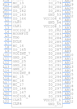
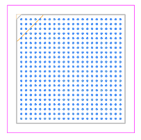
EP2C20F484I8N CAD Model
Symbol
Footprint
3D Model


EP2C20F484I8N Alternatives
EP2C20F256I8N – Same logic capacity, smaller 256-pin package
EP3C25F484I7N – Cyclone III alternative with higher performance and lower power
LFE2-20SE-5F484C (Lattice ECP2) – Comparable LE count, from Lattice Semiconductor
XC3S2000-4FG676C (Xilinx Spartan-3) – Similar density and performance in a competing architecture
ICE40HX8K-BG481I (Lattice iCE40) – Lower logic capacity but optimized for ultra-low power
EP2C20F484I8N Manufacturer
Intel Corporation is a global technology leader renowned for designing and manufacturing advanced semiconductor products that power the world’s computing and communications infrastructure. Headquartered in Santa Clara, California, Intel was founded in 1968 and is widely recognized for its pioneering role in developing microprocessors—the “brains” of modern computers. Beyond CPUs, Intel’s portfolio includes FPGAs, AI accelerators, chipsets, and connectivity solutions, serving diverse markets from data centers and PCs to automotive, IoT, and industrial systems. Through continuous innovation in process technology and system architecture, Intel drives digital transformation and enables breakthroughs in performance, power efficiency, and scalability.
EP2C20F484I8N FAQs
Question: Can the EP2C20F484I8N support differential I/O signaling standards like LVDS?
Answer: Yes, the device supports multiple differential I/O standards including LVDS, RSDS, and mini-LVDS, with programmable drive strength and termination options.
Question:What is the typical configuration time using Active Serial mode?
Answer: With a supported configuration clock of up to 20 MHz, configuration times are typically under 100 ms depending on the flash device and bitstream size.
Question:Is the EP2C20F484I8N suitable for use in automotive environments?
Answer: While it's industrial-grade, it can be used in non-safety-critical automotive subsystems like infotainment or driver information systems, but not in systems requiring AEC-Q100 certification.
Question:How does Cyclone II handle internal clock skew and timing optimization?
Answer: Cyclone II uses global, quadrant, and regional clock networks, along with dedicated PLLs, to manage low-skew clock distribution and phase alignment.
Question:Does this FPGA support soft-core processors like Nios II?
Answer: Yes, the EP2C20F484I8N supports Altera’s Nios II embedded processor, allowing users to implement fully customized SoC solutions directly within the FPGA fabric.


