

Ultra-practical PCB layout wiring rules
2024-09-02 17:50:11 1040
Layout
Component layout of the 10 rules:
- In accordance with the “first big and then small, first difficult and then easy” principle of layout, that is, the important unit circuits, core components should be prioritized layout.
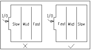
- Layout should refer to the schematic block diagram, according to the main signal flow law of the single board to arrange the main components.
- Components should be arranged to facilitate debugging and maintenance, that is, small components around the large components can not be placed, the need to debug the element, there should be enough space around the device.
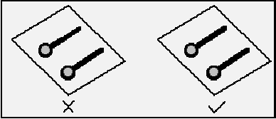
- The same structure of the circuit part, as far as possible, the use of “symmetrical” standard layout.
- Optimize the layout according to the standards of even distribution, balance of gravity, and beautiful layout;
- Plug-in components of the same type should be placed in one direction in the X or Y direction. Polarized discrete components of the same type should also strive to maintain consistency in the X or Y direction to facilitate production and inspection.
- Heat generating components should generally be evenly distributed to facilitate the heat dissipation of the single board and the entire machine, in addition to temperature detection components other than temperature-sensitive devices should be far away from the components that generate large amounts of heat.
- Layout should try to meet the following requirements: the total connecting lines as short as possible, the shortest key signal lines; high voltage, high current signals and small current, low voltage weak signals are completely separated; analog signals and digital signals are separated; high-frequency signals are separated from the low-frequency signals; high-frequency components should be adequately spaced.
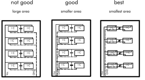
- 9.The layout of the decoupling capacitor should be as close as possible to the IC's power supply pins, and make the shortest loop formed between the power supply and ground.
- 10. The layout of components, should be given due consideration to the use of the same power supply devices as far as possible together, in order to facilitate the separation of power supply in the future.
Wiring
(1) Wiring priority
Key signal line priority: mapping small signals, high-speed signals, clock signals and synchronization signals and other key signals priority wiring
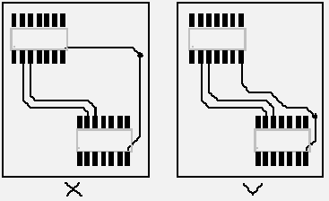
Density Priority Principle: Start wiring from the most complex devices connected to the single board. From the single board on the most dense wiring area to start wiring
Points to note:
- As far as possible for clock signals, high-frequency signals, sensitive signals and other key signals to provide a dedicated wiring layer, and to ensure that its minimum loop area. Manual prioritization of wiring, shielding and increased safety spacing should be taken when necessary. Ensure signal quality.
- The EMC environment between the power supply layer and the ground layer is poor, and the arrangement of interference-sensitive signals should be avoided.
- There are impedance control requirements of the network should be as long as possible according to the line length and width requirements of the wiring.
(2) Four specific alignment
1. Clock wiring:
Clock line is one of the factors that have the greatest impact on EMC. In the clock line should be less punched holes, try to avoid and other signal lines and walk the line, and should be away from the general signal line to avoid interference with the signal line. At the same time should avoid the power part of the board to prevent power and clock interference.
If the board has a specialized clock generator chip, the line should not be run underneath it, and copper should be laid underneath it, and if necessary, it can also be cut to the ground specifically for it. For many chips have reference crystal oscillators, these crystal oscillators should not be below the line, to lay copper isolation.
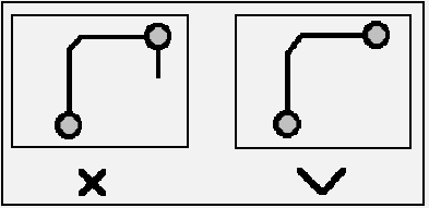
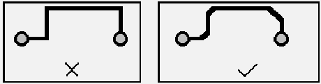
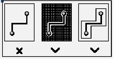
2. Right-angle alignment.
Right-angle alignment is generally required in PCB wiring to try to avoid the situation, but also almost become a measure of good or bad wiring one of the standards, then the right-angle alignment in fact, how much of an impact on signal transmission? In principle, right-angle alignment will make the line width of the transmission line changes, resulting in impedance discontinuity. In fact, not only the right-angle alignment, but also the Dunhuang, acute angle alignment may cause impedance changes.
Right-angle alignment of the impact on the signal is mainly reflected in three aspects:
First, the corner can be equated to a capacitive load on the transmission line, slowing down the rise time;
Second, the impedance discontinuity will cause signal reflection;
Third, the right-angle tip of the EMI generated.
3. Differential alignment.
Differential signals (Differential Signal) in the design of high-speed circuits in the application of an increasingly wide range of circuits in the most critical signals are often to use differential structure design. Definition: In layman's terms, it is the driver sends two equal and inverted signals, the receiver by comparing the difference between the two voltages to determine the logic state “0” or “1”. The pair of wires carrying differential signals is called differential wires.
Differential signals and ordinary single-ended signal alignment compared to the most obvious advantages are reflected in the following three aspects:
a. Strong anti-jamming ability, because the coupling between the two differential alignments is very good, when there is noise interference in the outside world, almost simultaneously coupled to the two lines, and the receiving end is only concerned about the difference between the two signals, so the outside world of the common-mode noise can be completely canceled out.
b. Can effectively inhibit EMI, the same reason, because the polarity of the two signals are opposite, they can cancel each other out of the electromagnetic field radiation, the tighter the coupling, the less electromagnetic energy leaked to the outside world.
c. Timing positioning accuracy, due to differential signal switching changes are located in the intersection of the two signals, rather than relying on ordinary single-ended signals, high and low two threshold voltage judgment, and therefore by the process, the temperature of the impact of the small, can reduce the timing error, but also more suitable for low-amplitude signals in the circuit. Currently popular LVDS (low voltage differential signaling) refers to this small amplitude differential signaling technology.
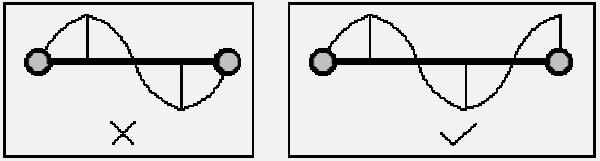
For PCB engineers, the most concerned or how to ensure that the actual alignment can fully play these advantages of differential alignment. Perhaps as long as the people who have contacted the Layout will understand the general requirements of differential alignment, that is, “equal length, equal distance”.
Equal length is to ensure that the two differential signals at all times to maintain the opposite polarity, reducing the common mode component; equal distance is mainly to ensure that the two differential impedance is the same, reducing reflections. “As close as possible to the principle” is sometimes one of the requirements of differential alignment.
4. Snake line.
Serpentine line is often used in the Layout of a class of alignment. Its main purpose is to adjust the delay, to meet the system timing design requirements.
The designer must first have this understanding:
Serpentine wire will destroy signal quality and change transmission delay, and should be avoided as much as possible when wiring. However, in actual design, in order to ensure that the signal has enough hold time, or to reduce the time offset between the same group of signals, often have to deliberately winding.
Caution:
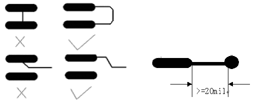
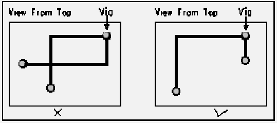
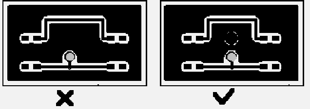
Differential signal lines appearing in pairs, generally parallel alignment, as little as possible through the hole, must be punched when the two lines should be punched together in order to achieve impedance matching.
A group of buses with the same attributes should be routed side by side as far as possible to achieve equal length. From the patch pads lead to the hole as far away from the pad.
(3) Wiring common rules
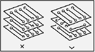
1. The direction of the alignment control rules:
That is, the direction of alignment of adjacent layers into an orthogonal structure. Avoid different signal lines in adjacent layers into the same direction to reduce unnecessary inter-layer interference;
When due to board structure limitations (such as some backplane) is difficult to avoid the situation, especially when the signal rate is high, should consider isolating the wiring layer with the ground plane, with the ground signal line to isolate the signal line.
2. The alignment of the open loop checking rules:
Generally do not allow one end of the floating wiring (Dangling Line), mainly to avoid the “antenna effect”, reduce unnecessary interference radiation and acceptance, otherwise it may bring unpredictable results.
3. Impedance matching check rules:
The wiring width of the same network should be consistent, changes in line width will cause uneven line characteristic impedance, when the transmission speed is higher will produce reflections, in the design should try to avoid this situation.
Under certain conditions, such as connector lead wires, BGA encapsulated lead wires similar structure, it may not be able to avoid changes in line width, should try to reduce the effective length of the middle inconsistent part.
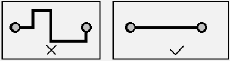
4. Alignment length control rules:
That is, the rule of short lines, in the design should try to make the wiring length as short as possible to reduce the interference problems caused by the alignment is too long, especially some important signal lines, such as the clock line, be sure to put its oscillator in a place very close to the device. For the case of driving multiple devices, it should be decided on a case-by-case basis what kind of network topology to use.
5. Chamfering rules:
PCB design should be avoided to produce sharp corners and right angles, resulting in unnecessary radiation, while the process performance is not good.
6. Device decoupling rules:
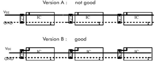
A. Add necessary decoupling capacitors on the printed board to filter out the interference signals on the power supply and make the power supply signal stable.
In the multilayer board, the location of the decoupling capacitor is generally not too demanding, but for the double-layer board, the layout of the decoupling capacitor and power supply wiring will directly affect the stability of the entire system, and sometimes even the success or failure of the design.
B. In double-layer board design, the current should generally be filtered by the filter capacitor before being used by the device.
C. In high-speed circuit design, the correct use of decoupling capacitors, the stability of the entire board.
7. Device layout partitioning/layering rules:
A. The main purpose is to prevent mutual interference between modules of different operating frequencies, and at the same time to minimize the wiring length of the high-frequency part.
B. For hybrid circuits, there are also analog and digital circuits are arranged on both sides of the printed circuit board, respectively, using different layers of wiring, the middle of the ground layer to isolate the way.
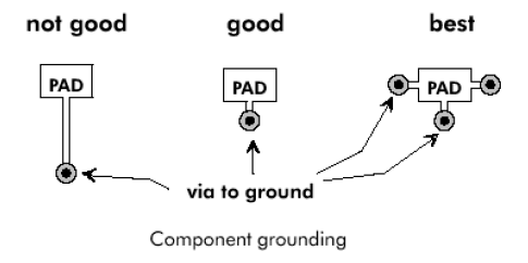
8. Ground loop rule:
Loop minimum rule, that is, the signal line and its circuit constitutes the ring area should be as small as possible, the smaller the ring area, the less radiation to the outside world, receiving the outside world interference is also smaller.
9. Integrity rules for power and ground layers:
For areas with dense conduction holes, care should be taken to avoid holes connecting with each other in the dug-out areas of the power and ground layers to form a division of the planar layer, thus destroying the integrity of the planar layer and consequently leading to an increase in the loop area of the signal line in the ground layer.
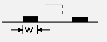
10. 3W rule:
In order to reduce crosstalk between the lines, should ensure that the line spacing is large enough, when the line center spacing is not less than 3 times the width of the line, then you can maintain 70% of the electric field does not interfere with each other, known as the 3W rule. If you want to achieve 98% of the electric field does not interfere with each other, you can use 10W spacing.
11. Shielding protection:
Corresponding to the ground loop rule, in fact, is also to minimize the signal loop area, mostly seen in some of the more important signals, such as clock signals, synchronization signals;
For some particularly important, particularly high-frequency signals, should consider the use of copper-axis cable shielding structure design, that is, the cloth line up and down the left and right ground line isolation, but also consider how to effectively make the shielding ground and the actual ground plane effectively combined.
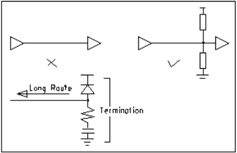
12. Alignment termination network rules:
In high-speed digital circuits, when the delay time of the PCB wiring is greater than 1/4 of the signal rise time (or fall time), the wiring can be viewed as a transmission line, in order to ensure that the input and output impedance of the signal and the transmission line impedance correctly matched, you can use a variety of forms of matching methods, the matching method selected with the network connection and the topology of the wiring.
A. For point-to-point connection (one output corresponds to one input), you can choose series matching at the beginning or parallel matching at the end. The former is simple and low-cost, but has higher latency. The latter has good matching effect, but the structure is complicated and the cost is high.
B. For point-to-multipoint (one output corresponds to multiple outputs) connection, when the topology of the network is a daisy chain, terminal parallel matching should be selected.
When the topology of the network is star structure, you can refer to the point-to-point structure. Star and daisy chain are the two basic topologies, other structures can be seen as a deformation of the basic structure, and some flexible measures can be taken to match.
In practice, we have to take into account the cost, power consumption and performance and other factors, generally do not pursue complete matching, as long as the mismatch caused by reflections and other interference is limited to an acceptable range.
13. Rules for closed-loop inspection of alignment:
Prevent signal lines from forming self-loops between different layers. In the multilayer board design is prone to such problems, since the loop will cause radiated interference.
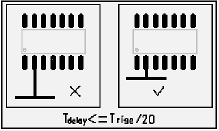
14. The alignment of the branch length control rules:
Try to control the length of the branch, the general requirement is Tdelay <= Trise/20.
15. The resonance of the alignment rules:
Mainly for high-frequency signal design, that is, the length of the wiring must not be an integer multiple of its wavelength, in order to avoid resonance phenomenon.
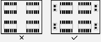
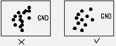
16. Isolated copper control rules:
The emergence of isolated copper, will bring some unpredictable problems, so the isolated copper and other signals connected to help improve the quality of the signal, usually isolated copper grounded or deleted.
In the actual production, PCB manufacturers will be some of the board of the vacant part of the increase in some copper foil, which is mainly to facilitate the processing of printed circuit boards, but also to prevent the printed circuit board warping also has a certain effect.
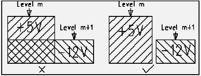
17. Overlapping power and ground layers rule:
Different power supply layers should avoid overlapping in space. Mainly to reduce the interference between different power supplies, especially some of the voltage difference between the power supply, the power supply plane overlap problem must try to avoid, difficult to avoid can be considered in the middle of the ground layer.
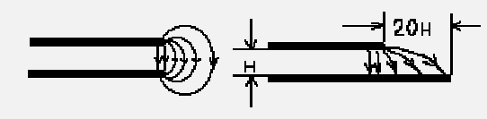
18. 20H rule:
As the power supply layer and the electric field between the ground layer is changing, the edge of the board will radiate electromagnetic interference to the outside. Known as the edge effect.
The solution is to shrink the power supply layer inward so that the electric field is conducted only within the confines of the ground layer. To a H (power and ground between the thickness of the medium) as a unit, if the shrinkage of 20H can be 70% of the electric field can be limited to the edge of the ground layer; shrinkage of 100H can be 98% of the electric field can be limited.
(4) Other
For single and double layer boards, power lines should be as thick and short as possible. The width of the power line and the ground line can be calculated according to the 1mm line width corresponding to the maximum current of 1A, power and ground loop as small as possible.
In order to prevent the coupled noise on the power line from entering the load device directly when the power line is long, the power supply should be decoupled before entering each device. And in order to prevent them from interfering with each other, the power supply of each load is independently decoupled and filtered before entering the load.
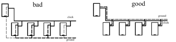
In the wiring should be kept well grounded. The following diagram shows the wiring rules for DDR.
DDR Wiring Rules
First of all, let's understand the composition of DDR2 signal:
The DDR2 chip model I used is: MT47H64M16HG
Package:
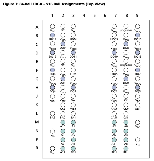
Pin definition:
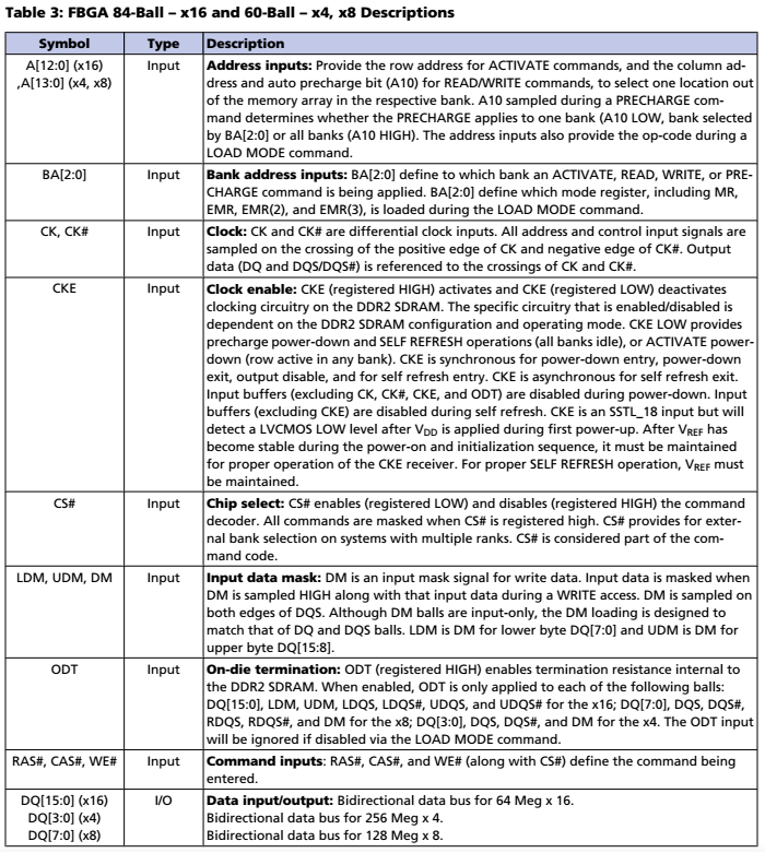
Schematic diagram:
Data lines and address lines:
Data lines: DQ[0-15], DQS, DM, (clock signal) CK/CK#.
Address lines: A[0-15], BA[0-2], (control signal) CS/WE/RAS/CAS, CKE, ODT


