

5CEFA7F23I7N FPGA: Features, Applications and Datasheet
2024-09-03 09:52:52 804
5CEFA7F23I7N Description
The 5CEFA7F23I7N is a FPGA (Field Programmable Gate Array) product from Intel (formerly Altera).FPGAs are highly flexible and customizable integrated circuits that allow users to define their internal logic functions by programming them after manufacturing.5CEFA7F23I7N features high performance, large memory and flexible programmability. It is widely used in data processing, communications, industrial automation, medical electronics and aerospace. It supports the implementation of complex logic and high-speed data processing, and is an important and indispensable part of modern electronic system design.
5CEFA7F23I7N Features
High performance: The 5CEFA7F23I7N features a high logic component count (~150,000 LE) and Adaptive Logic Modules (ALM), enabling it to handle complex logic tasks.
Large Memory: Rich embedded memory (7.696 Mbit) is built-in to support large data processing and caching needs.
Flexible and programmable: As an FPGA, the 5CEFA7F23I7N is highly flexible and programmable, allowing it to be configured and reprogrammed to meet specific user needs.
Wide Operating Temperature Range: Supports operation over a temperature range of -40°C to +100°C (or +85°C depending on the specific description) for a variety of harsh environments.
High-speed interfaces: Multiple I/O interfaces are provided to support high-speed data transmission and multiple communication protocols.
5CEFA7F23I7N Applications
Due to the high flexibility and customizability of FPGAs, 5CEFA7F23I7N is widely used in electronic systems requiring high performance, high reliability and programmability, such as data processing, communications, industrial automation, medical electronics, aerospace and other fields.
5CEFA7F23I7N Alternatives
Altera 5CEFA5F23I7N package type: FBGA-484。
5CEFA7F23I7N CAD Model
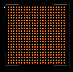
Footprint
5CEFA7F23I7N Manufacturer
Intel is one of the world's largest semiconductor chip makers, with a wide range of businesses covering a variety of areas including personal computers, data centers, the Internet of Things, artificial intelligence, and autonomous driving. In electronic components, Intel specializes in the design and production of high-performance processors, graphics processors, storage solutions, and other key components, providing innovative solutions and technical support to customers worldwide.
5CEFA7F23I7N FAQ
Question: Which family does the 5CEFA7F23I7N FPGA belong to, and what is its primary use?
Answer: The 5CEFA7F23I7N FPGA belongs to the Cyclone family from Intel (formerly Altera). This FPGA is widely used in many fields such as data processing, communications, and industrial automation because of its high performance, flexibility, and rich logic resources. It can be programmed according to specific needs to realize a variety of complex logic functions.
Question: What is the number of logic elements in a 5CEFA7F23I7N FPGA and how does this affect its performance?
Answer: The 5CEFA7F23I7N FPGA has approximately 150,000 Logic Elements (LEs), which are the basic building blocks inside the FPGA and are used to implement various logic functions. The greater the number of logic elements, the greater the complexity and parallelism that the FPGA can handle, thus improving its overall performance.
Question: What is the maximum operating frequency of the 5CEFA7F23I7N FPGA and what does this require of the design?
Answer: The 5CEFA7F23I7N FPGA can operate at a maximum frequency of 800 MHz (or different depending on the specific configuration). The high operating frequency means that the FPGA can accomplish more computational tasks in less time, but it also places higher demands on the timing and stability of the design. Designers need to carefully consider signal integrity and timing constraints to ensure that the FPGA operates stably at high frequencies.
Question: What is the package form factor of the 5CEFA7F23I7N FPGA and how does this affect the PCB design?
Answer: The 5CEFA7F23I7N FPGA is packaged in the FBGA-484 package form factor, which is a high-density, multi-pin package. This package form provides FPGAs with rich I/O interfaces and good heat dissipation performance, but it also poses higher challenges for PCB design. Designers need to carefully plan the PCB layout and wiring to ensure that the pins of the FPGA can be connected correctly and that the signal integrity and electromagnetic compatibility of the whole system are guaranteed.
Question: How do I program and configure the 5CEFA7F23I7N FPGA?
Answer: Programming and configuring the 5CEFA7F23I7N FPGA usually requires the use of Quartus Prime software provided by Intel (formerly Altera). This software provides a complete FPGA development flow from design input, simulation verification to programming download. Designers can write FPGA logic code in HDL (e.g., VHDL or Verilog) and then compile, simulate, and configure it using Quartus Prime. Finally, the configuration data is downloaded to the FPGA through the JTAG interface or a dedicated programmer to complete the entire programming process.


