

How to reduce parasitic capacitance in PCB layout?
2024-09-04 10:58:42 1059
Noise in electronic systems can take many forms. Whether it is picked up from an external source or passed between different areas of a PCB layout, noise can be picked up unintentionally in two ways: parasitic capacitance and parasitic inductance. Parasitic inductance is relatively easy to understand and diagnose, both from a crosstalk perspective and from the coupling of seemingly random noise between different parts of the board.
Dealing with parasitic capacitance is not necessarily more difficult, but it does require an understanding of how PCB layout geometry will affect inter-capacitance. In systems operating at high frequencies, or where high dV/dt nodes can create capacitive coupling noise, some simple PCB layout choices can help reduce parasitic components. In this article, a general description of how to reduce parasitic capacitance will be provided with some examples in high-frequency routing as well as in switching converters.
Identifying and Reducing Parasitic Capacitance
While there is no single formula for parasitic capacitance, there is a general definition:
- Parasitic capacitance is the unintended (usually undesired) capacitance that exists between two conducting structures separated by an insulator.
Sometimes this unintended capacitance is actually beneficial, in which case we do not use the word “parasitic” to describe it. Take the example of a power-ground plane pair; this simple structure helps provide a large charge reserve to support high-speed components with high input/output counts because of its inherent capacitance. Another example is in coplanar waveguides, where parasitic capacitance is essentially utilized to set the impedance of the interconnect to a desired value.
Parasitic capacitance can appear almost anywhere in a PCB. Take a look at the layout below; I've pointed out some areas where parasitic capacitance is evident. This only shows the capacitance generated by the top layer, but any layer can have capacitance.
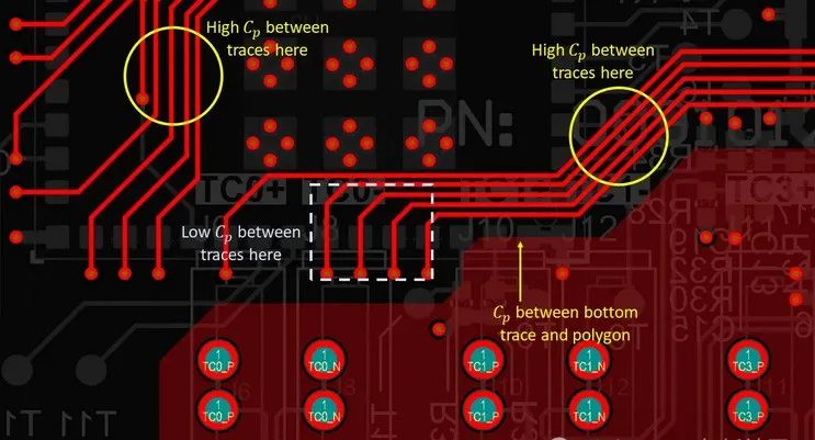
As the definition above implies, parasitic capacitance appears between any pair of conductors separated by a dielectric, and we can quickly identify multiple areas where parasitic capacitance appears in the above example. Whenever there is parasitic capacitance in a PCB layout, it can appear in two ways:
- As self-capacitance, it manifests itself as a high undesired capacitance between a conductor and a different conductor (usually GND).
- Mutual capacitance is the capacitance between two conductive structures that each refer to a third conductive structure; this is actually the form of capacitance that leads to capacitive coupling between two alignments.
Why is high parasitic capacitance important? It's important because whenever there is a varying potential between two capacitively coupled conductors, this causes some displacement current to flow on each conductor. This is a form of crosstalk that designers should be familiar with. Typically, we call it crosstalk when a switching signal induces its signal on the victim alignment, but the same mechanism can induce noise on any other structure in the presence of some parasitic capacitance.
While it can never be completely eliminated, in some cases it is beneficial to try to reduce it. To understand some strategies on how to reduce parasitic capacitance, it helps to look at some examples.
Example: High dV/dt node in a switching regulator
The regulator example section below shows the location of a strong dV/dt node and why this layout will have greater coupling into its feedback loop than to any nearby part of the system. In a switching regulator, the dV/dt node appears on the output of the switching stage, but before the rectifier/filter stage. In the example below, the SW_OUT node is our high dV/dt node, driven by the PWM signal.
This node has some parasitic capacitance to the nearby ground area. If there are other components or circuits nearby, the parasitic capacitance of those circuits can cause switching noise to appear in those circuits. The nearby ground has some help, but what really prevents noise coupling is the large capacitor that goes from SW_OUT back to the regulator chip. This large capacitor provides a low impedance path back to the high side of the switching stage for high dV/dt switching noise, effectively decoupling the output of the switching stage from GND.
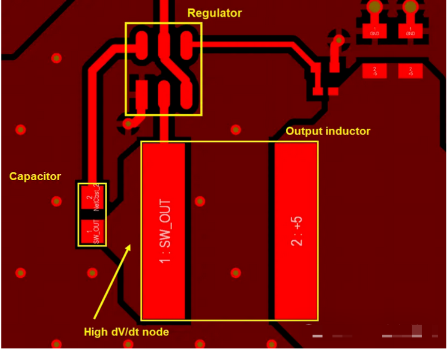
The dV/dt node can lead to noise coupling in the PCB layout. An intentionally placed capacitor prevents this!
Another strategy to reduce parasitic capacitance between SW_OUT and nearby alignments or circuits is to utilize the GND plane of the next layer. Placing the GND plane close to a high dV/dt node will reduce mutual capacitance by creating a stronger coupling of the electric field to the GND compared to certain other nodes in the PCB layout. In other words, a thinner dielectric layer between L1 and L2 of this board would be desired.
Example: Mutual capacitance between two alignments
Capacitive crosstalk is one of two types of coupling between alignments (the other being inductive), where a signal on one alignment can create noise on the other. At progressively higher frequencies, this is dominated by mutual capacitance. In a PCB layout, there are essentially two options for reducing this type of parasitic capacitance, assuming that the wiring has been routed over the GND region according to best practices:
- Bring the ground line closer to the signal line while keeping the impedance target the same and making the signal line narrower at the same time
- Increase the spacing between the signal lines
Almost any advice you can find on reducing crosstalk will recommend option #2, but in reality option #1 is just as effective. This is because it brings the mirrored charge/current in the ground plane closer to the signal lines. Operations like shorting the protected signal lines should not be attempted because it creates undesired parasitic capacitance on the ground and can actually increase crosstalk in some configurations.
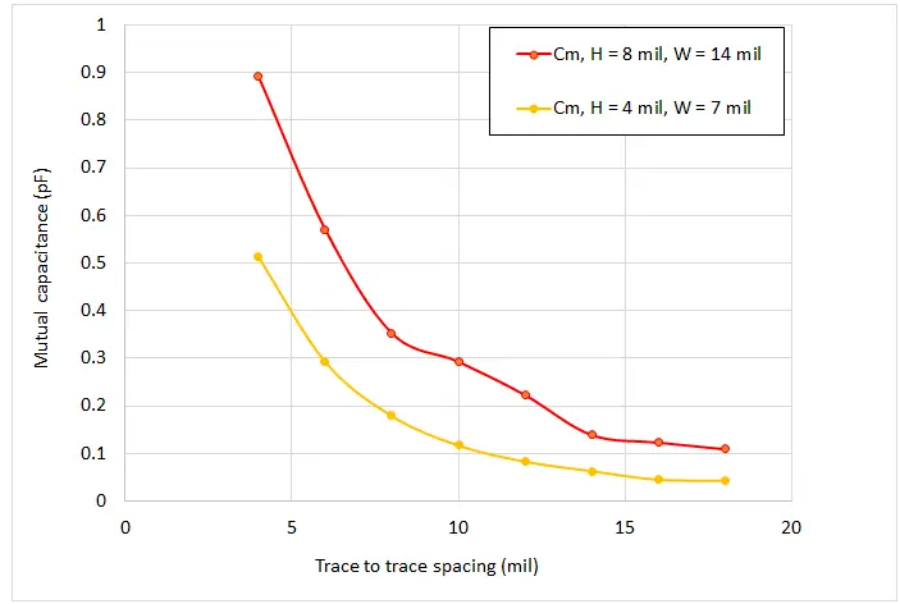
Simulation results show how the parasitic capacitance between two 50-ohm alignments is affected by the distance from the GND plane (noted as H).
For parasitic capacitance in the form of self-capacitance, the conductors need to be separated or made smaller. For parasitic capacitance in the form of mutual capacitance, the coupling needs to be reduced by increasing the self capacitance well beyond the mutual capacitance. In the above example, we see that simply by moving the ground plane closer to our mutual capacitance signal lines, their mutual capacitance is greatly reduced without any changes to the other conductors in the PCB layout.


