

How to Suppress SiC MOSFET Spikes Using a Buffering Circuit
2025-07-14 15:36:13 868
In recent years, the application scope of SiC MOSFETs as switching elements in various power supply applications and power lines has been expanding rapidly. One of the main reasons for this is that, compared to previous power semiconductors, SiC MOSFETs enable high-speed switching operations. However, due to the rapid changes in voltage and current during switching, the effects of the device's own package inductance and the parasitic inductance of the surrounding circuitry become significant, leading to large voltage spikes between the drain and source terminals. These spikes must not exceed the maximum specifications of the MOSFET being used, and various suppression methods exist for this purpose. In this application note, we will explain the design method for a buffer circuit, one of the techniques for suppressing drain-source voltage spikes.
Drain-Source Voltage Spike
The drain-source voltage spike is caused by the energy stored in the parasitic inductance of the lines and substrate routing during the Turn ON process, which resonates with the parasitic capacitance of the switching component.
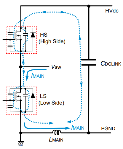
Figure. 1
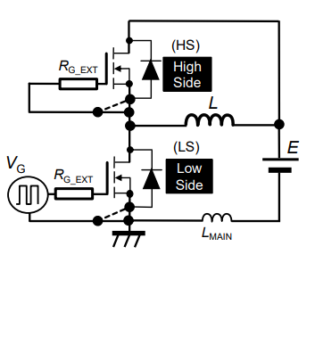
Figure 1 illustrates the ringing current path during spike generation. This figure shows the flow of the switching current IMAIN in a bridge structure composed of High-side (HS) and Low-side (LS) switching elements when the LS element turns on. This IMAIN typically flows from VSW through the wiring inductance LMAIN.
When the LS element turns off, the IMAIN flowing through LMAIN typically flows through the bulk capacitor CDCLINK connected between the input power supply HVdc-PGND, via the parasitic capacitance of the HS and LS elements as shown by the dashed lines in the figure. At this point, resonance occurs between LMAIN and the parasitic capacitance COSS (CDS+CDG) of the MOSFET on the LS side, resulting in a voltage spike between the drain and source terminals.
The maximum value of this spike, VDS_SURGE, is given by the following equation (*1), where VHVDC represents the voltage at the HVdc terminal, and ROFF represents the resistance of the MOSFET when it turns off.
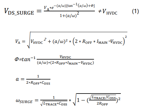
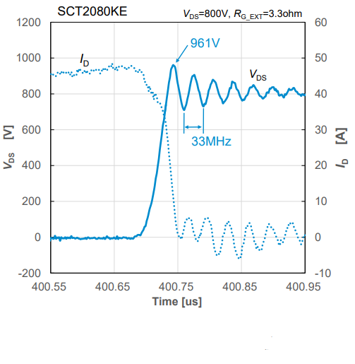
Figure. 2 Turn OFF voltage spike waveform
Figure 2 shows the voltage spike waveform during turn-off using a SiC MOSFET (SCT2080KE). When the HVdc voltage is 800V, VDS_SURGE is 961V, and the ringing frequency is approximately 33MHz. Using Equation (1), the LMAIN is calculated to be approximately 110nH based on this waveform.
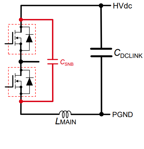
Figure 3. C buffer circuit
Next, a buffer circuit CSNB as shown in Figure 3 is added to the circuit. The Turn OFF voltage spike waveform with LMAIN removed is shown in Figure 4.
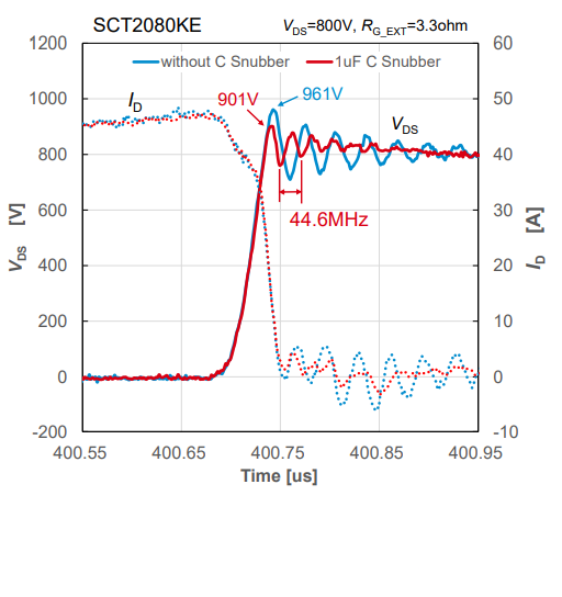
Figure 4. C buffer circuit reduces Turn OFF spike voltage
At this point, the voltage spike has decreased by over 50 V (approximately 901 V), and the ringing frequency has increased to 44.6 MHz, indicating that the LMAIN in the circuit network including CSNB has decreased. Similarly, using Equation (1), LMAIN is calculated to be approximately 71 nH. Ideally, the circuit layout should be designed to minimize wiring inductance; however, component heat dissipation design is typically prioritized, so the wiring layout may not be optimal. Therefore, by arranging buffer circuits as close as possible to the switching device to form a bypass circuit, the source of the voltage spike—wiring inductance—can be minimized, and the energy accumulated in the wiring inductance can be absorbed. This allows the voltage of the switching elements to be clamped, thereby reducing the Turn OFF voltage spikes.
Types and Selection of Buffer Circuits
Buffer circuits are categorized into passive circuits composed of resistors, inductors, and capacitors, and active circuits incorporating semiconductor components. (*1) This application note will explain circuit configurations that require no control and offer cost-effective solutions.
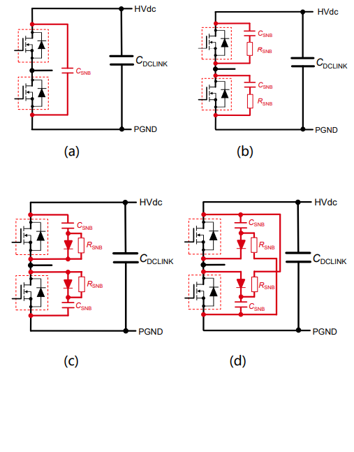
Figure. 5 Types of buffer circuits (a) C buffer circuit, (b) RC buffer circuit, (c) discharge type RCD buffer circuit, (d) non-discharge type RCD buffer circuit
Figure 5 shows examples of buffer circuits. The C buffer circuit (a) connects capacitors CSNB to the upper and lower parts of the MOSFET bridge structure, the RC buffer circuit (b) connects resistors RSNB and capacitors CSNB between the drain and source terminals of each switching element, and the RCD buffer circuit (c) adds a diode to the RC buffer circuit for discharge. and a non-discharge-type RCD buffer circuit (d) created by modifying the discharge path of the discharge-type RCD buffer circuit.
To maximize their effectiveness, these buffer circuits must be placed as close as possible to the switching elements.
(a) This configuration has fewer components but must be connected between the upper and lower parts of the bridge structure, resulting in longer wiring. Therefore, it is typically implemented using 2-in-1 discrete component modules rather than individual components.
(b) (b) Buffer circuits can be arranged near each switching element, but it must be ensured that all the energy accumulated in the CSNB is consumed by the RSNB each time the element turns on. Therefore, when the switching frequency increases, the power consumed by the RSNB may reach several watts, while the CSNB cannot be made very large, so the effect of suppressing spikes becomes limited. Additionally, the RSNB has limited spike absorption capacity, so the suppression effect is also constrained.
(c) The power consumed by RSNB in (c) is the same as in (b), but since the spike is absorbed only through a diode, the absorption effect is higher and more practical than in (b). However, attention must be paid to the recovery characteristics of the diode used, as the current changes significantly during spike absorption, and efforts must be made to minimize the wiring inductance of the buffer circuit. Additionally, if RSNB is connected in parallel with CSNB, the operational behavior is the same.
(d) The RSNB in (d) only consumes the voltage spike energy absorbed by the CSNB, and the energy accumulated by the CSNB is not fully released each time the switch is activated. Therefore, even if the switching frequency is increased, the power consumption of the RSNB does not become significantly larger, allowing the CSNB to be enlarged to greatly enhance the circuit's suppression effect. However, the circuit layout becomes complex, and if the substrate is not four layers or more, wiring becomes extremely difficult.
As described above, the buffer circuits introduced here each have their advantages and disadvantages, and the optimal buffer circuit must be selected based on the power supply circuit structure and power conversion capacity.
The following explains the design methods for each buffer circuit.
C Buffer Circuit Design
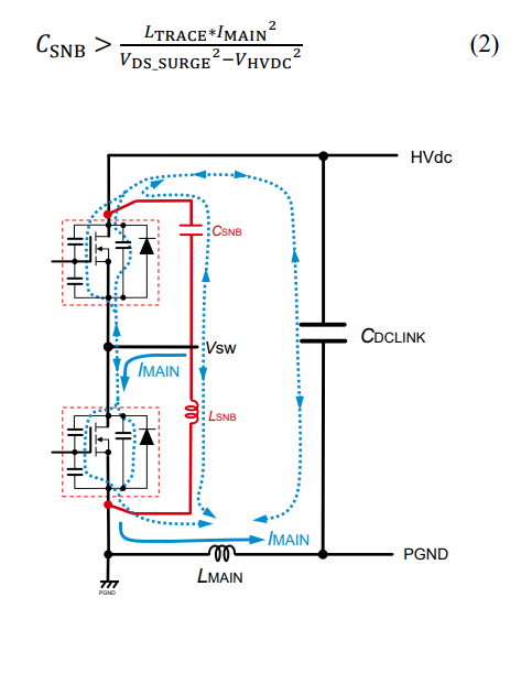
Figure. 6 C Buffer Circuit
The C buffer circuit shown in Figure 6 absorbs the energy accumulated in LMAIN through CSNB. Therefore, the LSNB formed in the buffer circuit must be smaller than LMAIN. Since the energy accumulated in CSNB is not discharged, the larger the capacitance, the better the voltage spike suppression effect. However, the equivalent series inductance (ESL) of the capacitor used must also be considered in LSNB. Generally, the larger the capacitor size, the larger the ESL, so care must be taken when selecting the capacitance.
To fully absorb the energy accumulated in LMAIN using CSNB, the capacitor must be selected based on the capacitance shown in Equation (2).
RC Buffer Circuit Design
Figure 7 shows the current path during operation of the RC buffer circuit.
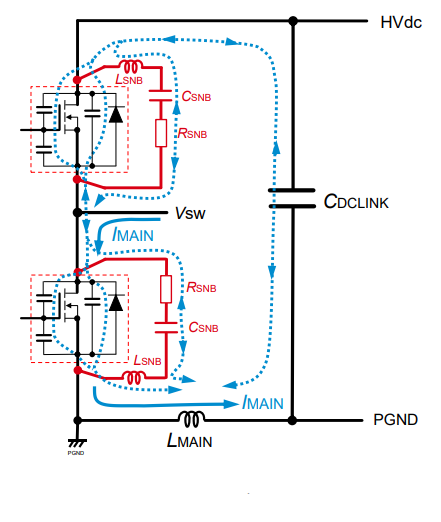
Figure. 7 RC Buffer Circuit
Like the C buffer circuit, the value of CSNB is determined by equation (2), while the reference value of RSNB is calculated using equation (3).
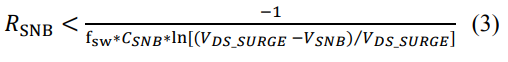
fSW: Switching frequency
VSNB: Discharge buffer voltage (0.9 times VDS_SURGE)
After determining RSNB, the power consumption of RSNB is calculated using Equation (4), and a resistor with sufficient power capacity is selected.
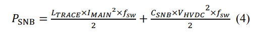
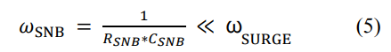
For the RC buffer circuit, Equation (4) includes an additional term because higher fSW or VHVDC results in greater power consumption by RSNB. If PSNB is too large, making resistor selection difficult, the capacitance value of CSNB must be reduced and recalculated. Additionally, to ensure the RC buffer circuit adequately absorbs voltage spikes, the resonant frequency ωSNB of RSNB and CSNB must be significantly lower than the resonant frequency ωSURGE of the voltage spike. This must be confirmed using the resonant frequency ωSNB of the RC buffer circuit shown in Equation (5).
Discharge-type RCD
Buffer circuit design The design of a discharge-type RCD buffer circuit is essentially the same as that of an RC buffer circuit. However, since the spikes are absorbed via a diode, there is no need to confirm the resonant frequency using equation (5). Additionally, the diode must be selected as a type with a small recovery current.
Non-discharge type RCD
Buffer circuit design The non-discharge type RCD buffer circuit differs from the discharge type RCD buffer circuit in that the power consumed by RSNB is limited to the energy of the voltage spike, and the selection range for RSNB used to suppress allowable losses is very broad. Therefore, the capacitance of CSNB can be increased to enhance the clamping effect.
CSNB is determined by equation (2), RSNB by equation (3), and the power consumption of RSNB by equation (6), without the second term involving CSNB and fsw from equation (4). Therefore, the increase in power consumption caused by the CSNB or fsw is negligible. A CSNB with a larger capacitance can be selected, which not only improves the clamping effect of the buffer circuit but also accommodates the high-frequencyization of fsw.
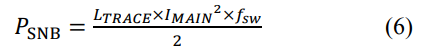
Figure 8 shows the discharge path when the non-discharge type RCD buffer circuit is operating. Since the peak of the upper arm is directed toward PGND and the peak of the lower arm is directed toward HVdc, the discharge current flows through RSNB and is less affected by line inductance. On the other hand, the wiring inductance LSNB between the drain and source of the MOSFET requires a small inductance value due to the large current changes.
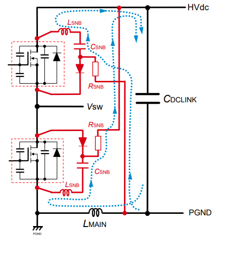
Figure. 8 Discharge of Non-Discharge Type RCD Buffer Circuit
Figure 9 shows the test circuit (a) and waveform (b) for verifying the effectiveness of the non-discharge RCD buffer circuit using the evaluation board (P02SCT3040KR-EVK-001), which employs a SiC MOSFET (SCT3080KR).
(a) Test Circuit
(b) Turn OFF s,b Waveform
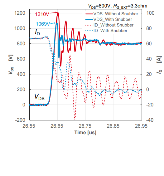
Figure 9. Turn OFF Voltage Spike Comparison (WithWithout Buffer Circuit)
The Turn OFF waveform when RG_EXT is 3.3Ω, HVdc is 800V, and drain current ID is approximately 70A.
When the buffer circuit is not connected, the voltage spike reaches as high as 1210V, but it is reduced to 1069V when the buffer circuit is added, a decrease of approximately 12%.
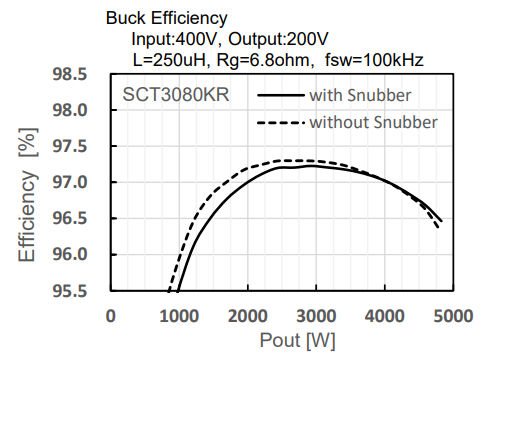
Figure. 10 Discharge of non-discharge type RCD buffer circuit
Figure 10 is a chart comparing the conversion efficiency of the Buck Converter. It shows the efficiency under the following conditions: input voltage 400V, output voltage 200V, RG_EXT 6.8Ω, and oscillation frequency 100kHz.
When the load power varies between 1kW and 4.8kW, the efficiency improves by up to 0.4% when no buffer circuit is used below approximately 4kW; On the other hand, when the load power exceeds 4 kW and a buffer circuit is present, the efficiency improves by 0.15%. This is because as the load power increases, the power loss caused by voltage spikes also increases, so the switching loss caused by the buffer circuit's spike suppression is reduced.
Differences in voltage spikes caused by different packaging
Finally, it should be noted that the Turn OFF spike varies depending on the packaging.
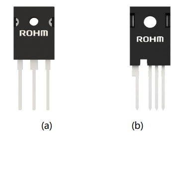
Figure. 11 SiC MOSFET packaging examples (a) TO-247N, (b) TO-247-4L
Figure 11 shows representative SiC MOSFET packages: (a) the widely adopted TO-247N (3L), and (b) the TO-247-4L, which has been increasingly adopted in recent years for drive circuits with a source terminal (i.e., the so-called Kelvin connection).
Compared to the 3L type, the 4L type alters the drive circuit path, thereby accelerating switching speed. As a result, both the Turn ON voltage spike and the Turn OFF voltage spike become larger.
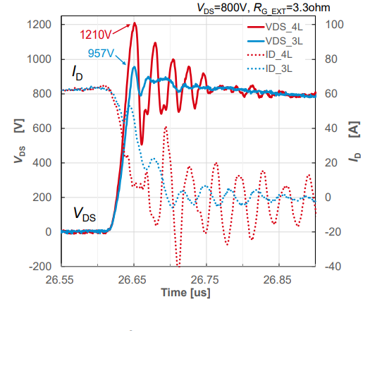
Figure. 12 Turn-off voltage spike comparison (TO-247N vs. TO-247-4L)
Figure 12 shows the comparison waveforms of the Turn OFF voltage spikes for the 3L type and 4L type. At VDS = 800V, RG_EXT = 3.3Ω, and ID = 65A, the Turn OFF waveform shows a drain-source voltage spike of 957V for the 3L type and 1210V for the 4L type.
As shown in Figures 7 and 8, the VDS ringing generated by this spike flows not only through CDS but also through CDG and CGS, causing unexpected voltage spikes in the MOSFET's gate-source voltage (VGS) and potentially exceeding the VGS specification. The method for suppressing VGS voltage spikes is described in another application note (*2). When the suppression effect of the method recorded in that note is insufficient, adding a buffer circuit between the drain and source terminals is also an effective means of suppressing VGS spikes.
As described above, the gate signals of MOSFETs in a bridge circuit are interrelated and operate between MOSFETs, generating unexpected voltage spikes between the gate and source terminals. The suppression methods require consideration of the substrate's circuit layout and should be adapted based on the specific circumstances. We hope this article serves as a useful reference and is utilized flexibly.


