

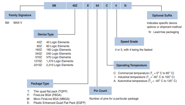
5M80ZM64I5N CPLDs: Features, Applications and Alternatives
2025-04-22 10:33:35 1265
5M80ZM64I5N Description
The 5M80ZM64I5N is a low-power, high-performance CPLD (Complex Programmable Logic Device) from Intel's MAX® V family, designed to deliver optimal logic density, non-volatile storage, and instant-on functionality. With 80 logic elements, it is housed in a 64-pin QFP package and operates across the industrial temperature range. This device is ideal for replacing traditional glue logic and enabling simple control and interface functions in embedded systems.
5M80ZM64I5N Features
Logic Elements (LEs):
Contains 80 logic elements, ideal for simple control, interface, and glue logic applications.
Non-Volatile Flash-Based Architecture:
Enables instant-on capability with no need for external configuration memory.
Ultra-Low Power Consumption:
Typical static power consumption in the range of microwatts, making it perfect for battery-powered or energy-sensitive applications.
User Flash Memory (UFM):
8 Kbits of on-chip user flash memory for storing system data, device settings, or calibration constants.
Package Type:
Comes in a compact 64-pin QFP (M64) package for space-constrained applications.
I/O Capability:
Provides up to 54 user I/O pins, configurable for various voltage standards and protocols.
Wide Operating Temperature Range:
Rated for industrial temperature (-40°C to +100°C), suitable for rugged environments.
On-Chip Oscillator:
Internal oscillator (~8 MHz) available for timing and control tasks.
JTAG Programming and Boundary Scan Support:
Supports in-system programming and full boundary-scan testing, enhancing development and testability.
Fast Setup and Hold Times:
Short propagation delays and setup times for responsive logic execution.
RoHS-Compliant & Pb-Free:
Environmentally friendly and compliant with global regulatory standards.
Integrated Power-On Reset (POR):
Ensures the CPLD starts up reliably and in a known state.
5M80ZM64I5N Applications
Industrial automation control units
Portable medical and monitoring devices
Simple bridging or glue logic between peripherals
Board-level configuration control
Power management sequencing
Consumer electronics (e.g., TV or printer control logic)
Communication infrastructure (e.g., status LED control, reset logic)
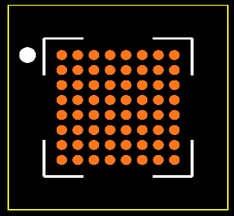
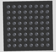
5M80ZM64I5N CAD Model
Footprint
3D Model

5M80ZM64I5N Alternatives
Here are some comparable alternatives to consider based on performance and pin count:
5M80ZT100I5N – Same logic capacity in a TQFP-100 package
XC2C64A-6TQG144C – Xilinx CoolRunner-II CPLD with 64 macrocells
ATF1508ASV-15JU84 – Microchip CPLD with 128 macrocells, suitable for more complex logic
5M160ZM64I5N – MAX V with higher logic capacity (160 LEs) in same package
LCMXO2-1200HC-4TG100I – Lattice MachXO2 device, higher logic and more I/Os
5M80ZM64I5N Ordering Information
5M80ZM64I5N FAQs
Question: Can the 5M80ZM64I5N operate without an external configuration memory?
Answer: Yes, it uses internal non-volatile flash memory, enabling instant-on operation without external configuration.
Question: Is the 5M80ZM64I5N programmable via JTAG?
Answer: Absolutely, it supports in-system programming and boundary-scan testing using the standard JTAG interface.
Question: What is the maximum number of user I/O pins available?
Answer: It offers up to 54 user I/Os, depending on configuration and pin multiplexing.
Question: How much user flash memory (UFM) does this device include?
Answer: It provides 8 Kbits of UFM, allowing for parameter storage, calibration values, or small datasets.
Question: What is the internal oscillator frequency of the MAX V CPLDs?
Answer: The internal oscillator runs at approximately 8 MHz, but this can vary slightly across devices.


