

EP3C10F256I7N FPGAs: Features, Applications and Datasheet
2025-03-24 14:25:05 1493
EP3C10F256I7N Description
The EP3C10F256I7N is a Cyclone® III FPGA from Intel (formerly Altera), designed for low power, cost-effective applications while maintaining high performance. Packaged in a 256-pin FineLine BGA (FBGA), this device features 10,320 logic elements and supports a variety of I/O standards, suitable for general-purpose logic, data processing, and control applications.
EP3C10F256I7N Features
Logic Elements: 10,320 LEs
Memory: 414 Kbits of embedded memory
I/O Pins: 182 maximum user I/Os
Package: 256-pin FBGA (17x17 mm)
Speed Grade: Industrial temperature range (I), speed grade 7 (slowest, low-power variant)
PLL Support: 2 embedded PLLs
Low Power Consumption: Static power as low as 0.25W
Voltage Supply: Core voltage 1.2V; I/O banks support 1.2V, 1.5V, 1.8V, 2.5V, 3.3V
Configuration: Supports multiple methods including JTAG, AS, and PS configuration
RoHS Compliant and suitable for environmentally conscious applications
EP3C10F256I7N Applications
Industrial control systems
Medical equipment
Wireless communication base stations
Automotive electronics (non-safety critical)
Consumer electronics
Video and image processing
Motor control and automation
Data acquisition and sensor interface systems
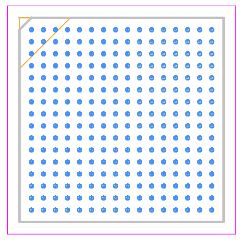
EP3C10F256I7N CAD Model
Symbol
Footprint
3D Model

EP3C10F256I7N Alternatives
EP3C16F256I7N: This is from the same Cyclone III family but offers a higher logic element (LE) count of 15,408, providing more processing capacity for complex designs while retaining the same package.
EP2C8Q208C8N: From the older Cyclone II generation, this part offers slightly fewer logic elements and older architecture. It's a potential lower-cost option for legacy systems.
XC6SLX9-2TQG144C by AMD Xilinx: A comparable device from the Spartan-6 family, this FPGA offers a similar logic element count and is suitable for applications requiring Xilinx toolchains or features like integrated DSP slices.
LFE3-17EA-6FN484I by Lattice Semiconductor: A higher-end device from the ECP3 family, it offers more SERDES channels and is suited for applications needing advanced I/O or networking features.
10CL010YU256I7G by Intel: From the newer Cyclone 10 LP family, this FPGA offers improved power efficiency, making it a good choice for designs prioritizing low power consumption with comparable logic capacity.
EP3C10F256I7N Manufacturer
Intel Corporation is a global technology leader headquartered in Santa Clara, California, known for designing and manufacturing advanced semiconductor products. Founded in 1968, Intel is best known for its microprocessors that power a majority of the world’s computers. The company also develops FPGAs, chipsets, networking solutions, and AI accelerators, playing a key role in data centers, PCs, and embedded systems. Intel continues to drive innovation across computing, connectivity, and cloud infrastructure.
EP3C10F256I7N FAQs
Q: Can EP3C10F256I7N's internal memory blocks operate simultaneously at different clock domains without PLL synchronization?
A: Yes, the M9K memory blocks in the Cyclone III architecture support true dual-port operation, allowing independent clock domains, but caution is needed for metastability and latency management.
Q: What is the recommended strategy for minimizing startup current spikes during configuration?
A: Use soft-start features in the power supply and avoid simultaneous power-up of I/O banks; stagger supply rails if using multiple regulators to limit inrush.
Q: Does EP3C10F256I7N support hot-socketing on all I/O banks?
A: No, while certain I/O banks tolerate hot insertion, Altera recommends isolating or buffering hot-socketed signals to avoid damage or unpredictable behavior.
Q: How does the speed grade (7) impact maximum toggle frequency of logic elements and I/O compared to speed grade (6)?
A: Speed grade 7 FPGAs exhibit approximately 10–15% lower maximum toggle frequency and higher internal propagation delay than speed grade 6, impacting high-speed designs.
Q: What is the total maximum simultaneous switching output (SSO) per bank to avoid signal integrity issues?
A: Depending on I/O standard and drive strength, Cyclone III recommends limiting SSO to around 16–24 pins per bank to avoid simultaneous switching noise and ground bounce.


