

EP3C5F256C8N FPGAs: Features, Applications and Datasheet
2025-01-07 10:28:48 1357
EP3C5F256C8N Description
The EP3C5F256C8N is an FPGA (Field Programmable Gate Array) from the Altera Cyclone III family, designed for low-cost and low-power applications. It offers a balance of cost-effectiveness, performance, and resource availability, making it ideal for a wide range of applications requiring programmable logic.
EP3C5F256C8N Features
Logic Elements (LEs): 5,136 LEs, optimized for high-density applications.
Memory: 89 Kbits of embedded RAM for data storage and buffering.
I/O Pins: 156 user-configurable I/O pins for interfacing with peripherals.
Clock Management: PLLs (Phase Locked Loops) for clock management and synchronization.
Package Type: Available in a compact 256-pin FBGA package.
Operating Voltage: Core voltage of 1.2V with I/O voltage options from 1.2V to 3.3V.
Power Consumption: Designed for low-power consumption to suit energy-efficient applications.
Temperature Range: Supports an industrial temperature range of -40°C to +100°C.
Design Tools: Fully supported by Intel Quartus Prime software for design implementation.
EP3C5F256C8N Applications
Consumer Electronics: Used in devices such as gaming systems, digital cameras, and set-top boxes.
Telecommunications: Ideal for base stations, network infrastructure, and communication systems.
Industrial Automation: Utilized in control systems, robotics, and sensor interfacing.
Medical Devices: Suitable for imaging systems and portable diagnostic equipment.
Automotive Electronics: Used in infotainment systems and advanced driver-assistance systems (ADAS).
Educational and Prototyping Projects: For training and experimentation in digital design.
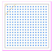
EP3C5F256C8N CAD Model
Symbol
Footprint
3D Model


EP3C5F256C8N Alternatives
EP3C10F256C8N: Offers higher logic element capacity and more memory for larger designs.
EP2C5F256C8N: A predecessor with similar features but fewer resources.
Xilinx Spartan-6 XC6SLX9-2FTG256C: Comparable FPGA from Xilinx, offering similar logic and I/O capabilities.
Lattice MachXO3LF-6900C: A low-cost alternative from Lattice Semiconductor.
Intel MAX 10 Series: Integrated flash-based FPGAs with enhanced features for small-scale designs.
EP3C5F256C8N Manufacturer
Intel Corporation, founded in 1968, is a global leader in semiconductor innovation and technology. Renowned for its development of microprocessors, Intel powers computing devices across industries, from personal computers to data centers. The company is at the forefront of advancements in artificial intelligence, 5G, and autonomous systems, offering processors, memory, and software solutions. Headquartered in Santa Clara, California, Intel is committed to delivering high-performance, energy-efficient products that drive technological progress and enable digital transformation worldwide. Its continuous innovation shapes the future of computing and connectivity.
EP3C5F256C8N FAQs
What is the maximum operating frequency of the EP3C5F256C8N?
The maximum operating frequency depends on the specific design and application, but the FPGA typically supports clock frequencies up to 150 MHz or higher, depending on the timing constraints and logic complexity.
How many PLLs (Phase Locked Loops) are available in the EP3C5F256C8N?
The EP3C5F256C8N has two PLLs, which can be used for clock management, frequency synthesis, and phase shifting in your design.
What is the total amount of embedded memory in the EP3C5F256C8N?
The FPGA includes 89 Kbits of embedded RAM, which can be utilized for data buffering, storage, or creating custom memory blocks.
What is the power consumption of the EP3C5F256C8N under typical operating conditions?
The power consumption depends on the utilization of logic, I/O, and clock resources. For typical designs, the EP3C5F256C8N is considered low-power, with a core voltage of 1.2V and I/O voltage ranging from 1.2V to 3.3V.
What types of I/O standards are supported by the EP3C5F256C8N?
The EP3C5F256C8N supports various I/O standards, including LVTTL, LVCMOS, PCI, SSTL, and HSTL, allowing seamless interfacing with a wide range of peripherals and devices.


