EPM570F100C5N CPLDs: Features, Applications and Datasheet
2025-02-20 10:06:09 1104
EPM570F100C5N Description
The EPM570F100C5N is a member of the MAX V series of field-programmable gate arrays (FPGAs) from Intel (formerly Altera). This FPGA is designed to provide low-power, high-performance capabilities, making it suitable for various industrial, automotive, consumer electronics, and communications applications. It features an architecture that offers a combination of logic elements, memory resources, and I/O capabilities while consuming low power, which is essential for many portable and battery-operated devices.
EPM570F100C5N Features
High Density Logic Elements: The EPM570F100C5N comes with 5,000 logic elements, offering significant capacity for a wide range of applications.
Configurable I/O: It supports a wide variety of I/O standards, ensuring compatibility with different communication protocols.
Low Power Consumption: Designed for low power, the FPGA is optimized to meet power efficiency requirements, ideal for battery-operated devices.
Integrated Memory Blocks: It includes internal memory resources, such as block RAM, which are useful for buffering and temporary data storage in embedded systems.
Flexible Clocking: The FPGA supports a variety of clock sources and configurations to meet the timing requirements of different applications.
Programming: The device is programmed via JTAG, and can be reconfigured multiple times, providing flexibility in design and field updates.
Secure Design: It offers a secure configuration to protect against unauthorized access or tampering of the design.
EPM570F100C5N Applications
Consumer Electronics: Ideal for applications in smart home devices, portable devices, and wearables where low power consumption and flexibility are crucial.
Automotive: Suitable for infotainment systems, advanced driver assistance systems (ADAS), and communication systems in vehicles.
Industrial Automation: Used in embedded control systems, sensor interfaces, and factory automation where reconfigurability and low power are important.
Telecommunications: Applied in communications devices such as routers, switches, and base stations.
IoT (Internet of Things): Perfect for IoT applications where low power and efficient processing are necessary.
Embedded Systems: Used in various embedded applications that require programmable logic to meet specific tasks, from data processing to communication.
EPM570F100C5N CAD Model
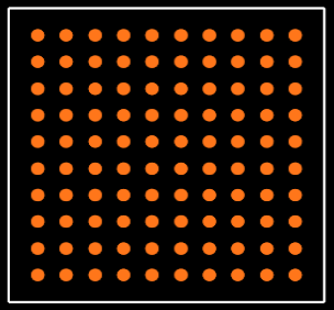
Footprint

EPM570F100C5N Alternatives
Xilinx Spartan-6 FPGAs: Similar in terms of power efficiency and low cost for applications requiring moderate logic capacity.
Lattice iCE40 FPGAs: Known for ultra-low power and compact design, useful for battery-powered devices.
Intel MAX 10 FPGAs: Another low-power FPGA from Intel designed for similar applications, with a focus on automotive, industrial, and IoT systems.
Microsemi IGLOO2 FPGAs: Low-power FPGAs designed for embedded systems, with strong focus on security and efficiency.
Actel ProASIC3 FPGAs: These offer a balance between low power consumption and high-performance features, typically used in industrial and automotive sectors.
EPM570F100C5N FAQs
How to program the EPM570F100C5N FPGA?
The EPM570F100C5N FPGA is programmed using JTAG programming tools, such as the USB-Blaster or ByteBlaster. Configuration files in .sof (SRAM Object File) format are used for the programming.
How do I achieve low power operation in the EPM570F100C5N?
You can achieve low power operation by optimizing clocking resources, using low power I/O standards, and employing dynamic power management techniques, such as clock gating and resource optimization.
How to interface with external devices using EPM570F100C5N?
The FPGA offers a wide range of configurable I/O options, allowing you to interface with external devices like sensors, actuators, and other embedded systems via GPIO, SPI, UART, or other communication protocols.
How can I use the internal memory of EPM570F100C5N?
The EPM570F100C5N includes block RAM that can be used for data buffering or temporary storage. You can configure the memory blocks as dual-port RAMs, FIFOs, or other memory structures to fit your application.
What is the maximum clock frequency supported by the EPM570F100C5N?
The EPM570F100C5N supports a maximum clock frequency of 200 MHz, but this can depend on the design's complexity and the constraints on the FPGA’s resources.


