

Gallium Nitride Offers Powerful Solutions in High Voltage Applications
2024-09-06 10:41:27 615
In the field of electrical engineering, the trend toward higher operating voltages is driven by the need for increased efficiency and power density in a variety of applications. Gallium Nitride (GaN) technology is emerging as a powerful solution to meet these needs.
In industrial environments, internal voltage rails are also moving up. These higher voltages are critical for delivering higher power in applications such as motor drives, compressors and large HVAC systems.
Rapidly growing consumer and industrial sectors in emerging economies are challenged by grid instability. Voltage fluctuations and line swells, often exacerbated by aging infrastructure, pose a significant threat to electronic systems.
Challenges of Silicon Devices in High Voltage Environments
All power devices have defined operating limits. For example, a 725 V silicon MOSFET can typically operate safely up to 650 V and derate to 725 V. Prolonged exposure to voltages higher than 725 V can lead to avalanche breakdown, resulting in localized heating and potential structural damage. Voltage spikes (such as lightning strikes or power supply wiring errors) and line swells due to grid instability can push these devices to their limits, leading to catastrophic failures.
Energy Loss - Gallium Nitride vs. Silicon
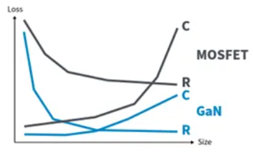
R = Conduction Loss - RDS(ON)
C = Switching Losses - COSS
Advantages of PowiGaN Technology in High Voltage Applications
In contrast, PowiGaN devices do not exhibit the avalanche breakdown mechanism inherent in silicon devices. Their internal cascade structure and high breakdown voltages (typically more than twice the rated voltage) allow them to withstand high voltage spikes and long-term line swell. These devices temporarily increase resistance during voltage spikes, reducing efficiency slightly, but recover quickly without significant impact on performance. Even under multiple spiking events or prolonged swell, PowiGaN devices maintain safe and efficient operation without degradation.
PowiGaN's role in future high-voltage applications
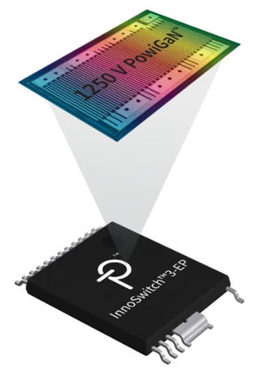
Power Integrations' recently introduced 1250 V PowiGaN device marks an important advancement. The devices allow 1000 V peak operation with significant derating, providing robust protection against grid instability and power disturbances. These devices are now moving into an area traditionally dominated by silicon carbide (SiC) devices, expanding their range of applications.
In summary, PowiGaN technology offers significant advantages in the face of grid instability in the current market. It ensures high-quality, reliable products in an expanding consumer market. In addition, PowiGaN's robust cascade structure and potential for higher voltage applications make it a key player in the future of power electronics.


