

IBM unveils key breakthrough in optics, ushering in the “speed of light era” for generative AI
2024-12-13 11:00:52 1496
New optoelectronic co-packaging technology may replace electrical interconnects in data centers, dramatically increasing the speed and energy efficiency of AI and other computing applications
BEIJING, Dec. 12, 2024 /PRNewswire/ -- IBM (NYSE: IBM) recently unveiled its breakthrough research in optics technology that promises to dramatically improve the efficiency of training and running generative AI models in data centers.The next-generation photovoltaic co-packaged optics (CPO) process, developed by IBM researchers, uses optics technology to enable the use of electrical interconnects within data centers. IBM researchers have developed a next-generation co-packaged optics (CPO) process that enables light-speed connectivity within data centers through optics, complementing existing short-distance fiber optic cables. By designing and assembling the first declared successful polymer optical waveguide (PWG), IBM researchers are demonstrating how co-packaged optics will redefine the computing industry's high-bandwidth data transfer between chips, boards and servers.
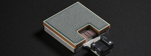
Figure. 1 IBM optics module
Today, fiber-optic technology is widely used for high-speed data transmission over long distances, enabling “light instead of power” to manage virtually all commercial and communications transmissions worldwide. While data centers have adopted fiber optics for their external communications networks, their internal racks still communicate primarily with copper wires. GPU gas pedals connected by wires can sit idle more than half the time, waiting for data from other devices during large distributed training sessions, resulting in high costs and wasted energy.
IBM researchers have found a new way to bring the speed and capacity of optics into the data center. In one of its latest publications, IBM demonstrated its world-first, optoelectronic co-packaging prototype that enables high-speed optical connectivity. This technology could dramatically increase communication bandwidth in data centers, minimizing GPU downtime while dramatically speeding up AI. This innovation will enable the following new breakthroughs:
Reduce the cost of generative AI at scale: Reduce energy consumption by more than 5x compared to medium-distance electrical interconnects,[1] while extending data center interconnect cable lengths from 1 meter to hundreds of meters.
Increased AI model training speed: training large language models is nearly five times faster with optoelectronic co-packaging compared to traditional wires, reducing training time for standard large language models from three months to three weeks; for larger models and more GPUs, performance gains will be even greater. [2]
Dramatically improve data center energy efficiency: with the latest photovoltaic co-packaging technology, each AI model trained saves as much power as the combined annual power consumption of 5,000 U.S. homes. [3]
Dario Gil, senior vice president of IBM and president of IBM Research, said: “Generative AI requires more and more energy and processing power, and data centers must be upgraded accordingly, and photovoltaic co-packaging technology can help data centers to face the future with ease. With the breakthrough in optoelectronic co-encapsulation technology, fiber optic cables will dramatically improve data transmission efficiency in data centers, and inter-chip communication and processing of AI workloads will also be more efficient, and we will enter a new era of high-speed, more sustainable communications.”
80x faster bandwidth than existing inter-chip communications
Thanks to advances in chip technology in recent years, more and denser transistors can be accommodated on a chip; for example, IBM's 2-nanometer chip technology can implant more than 50 billion transistors on a single chip. Optical co-packaging technology is designed to expand the density of interconnections between gas pedals, helping chipmakers add optical pathways connecting chips to electronic modules, thereby exceeding the limitations of existing electronic pathways. the new high-bandwidth-density optical structures described in the IBM paper, along with other innovations, such as transmitting multiple wavelengths per optical pathway, hold the promise of increasing bandwidth for inter-chip communications up to 80 times that of a wired connection.
Compared to the most advanced optoelectronic co-packaging technology, IBM's innovations enable chipmakers to add six times the number of optical fibers to the edge of a silicon photonic chip, the so-called “sideburn density (beachfront density)”. Each fiber is about three times as wide as a strand of hair, ranging in length from a few centimeters to several hundred meters, and capable of transmitting trillions of bits of data per second. the IBM team used a standard encapsulation process to encapsulate high-density polymer-based optical waveguides (PWGs) in 50-micron spaced optical channels and adiabatically coupled them to the silicon photonic waveguides.
The paper also notes that the aforementioned optoelectronic co-packaged modules with 50-micron pitch polymer PWGs passed all the stress tests required for manufacturing for the first time. The modules were subjected to high humidity environments, temperatures ranging from -40°C to 125°C, and mechanical endurance tests to ensure that the optical interconnects would not break or lose data, even if bent. In addition, the researchers demonstrated 18-micron pitch polymer optical waveguide technology: four polymer optical waveguide devices stacked together can achieve up to 128 channels of connectivity.
IBM continues to lead semiconductor technology development
In the face of growing AI performance demands, optoelectronic co-packaging technology opens up a new communication pathway and may replace off-module communication from electronics to optics. This technology breakthrough continues IBM's leadership in semiconductor innovation, including the world's first 2nm chip technology, the first 7nm and 5nm process technologies, nanosheet transistors, vertical transistors (VTFETs), single-chip DRAMs and chemically amplified photoresists.
The project was designed, modeled and simulated in Albany, N.Y., and prototype assembly and module testing was performed at IBM Labs in Bromont, Quebec, Canada, one of the largest chip assembly and test facilities in North America.
[1] Reduced from 5 microJoules per bit to less than 1 microJoule. [2] Data is based on training of a 70 billion parameter large language model using industry standard GPUs and interconnects. [3] Data based on training of very large large language models such as GPT-4 using industry standard GPUs and interconnects.
About IBM
IBM is the world's leading provider of hybrid cloud, artificial intelligence and enterprise services, helping clients in more than 175 countries and territories derive business insights from the data they own, streamline business processes, reduce costs and gain a competitive advantage in their industries. More than 4,000 government and business entities in critical infrastructure sectors such as financial services, telecommunications and healthcare rely on the IBM Hybrid Cloud Platform and Red Hat OpenShift to quickly, efficiently and securely enable digital transformation.IBM's groundbreaking innovations in artificial intelligence, quantum computing, industry cloud solutions, and enterprise services provide our clients with open and flexible choices. A long-term commitment to corporate integrity, transparent governance, social responsibility, a culture of inclusion and a spirit of service are the cornerstones of IBM's business.


