

Intel Foundry Direct Connect 2025: Advancing 14A and 18A Technologies, Strengthening Ecosystem Partnerships
2025-04-30 10:47:17 1433
Today, the 2025 Intel Foundry Direct Connect kicked off with Intel sharing the latest advances in multi-generation core process and advanced packaging technologies, and announcing new ecosystem programs and partnerships. Also, industry sectors convened to discuss how Intel's system-level foundry model fosters synergies with partners to help customers advance innovation.
In his opening remarks, Intel CEO Lip-Bu Tan discussed Intel Foundry's progress and future development priorities, highlighting that the company is driving its foundry strategy into the next phase. Keynote addresses were also given by Kevin O'Buckley, General Manager, Foundry Services, and Naga Chandrasekaran, Chief Technology and Operations Officer, Intel Foundry. They highlighted the company's diverse global manufacturing and supply chain footprint, as well as the ecosystem support, and showcased the most recent developments in process and advanced packaging. The ecosystem support of the business.
In his introductory remarks, Lip-Bu Tan was joined by ecosystem partners Synopsys, Cadence, Siemens EDA, and PDF Solutions, who emphasized cooperation in providing foundry clients with services. Executives from Qualcomm, Microsoft, and MediaTek joined O'Buckley.
Intel is committed to establishing a world-class foundry to address the expanding need for leading-edge process technologies, innovative packaging and manufacturing,” said Lip-Bu Tan, CEO of Intel Corporation. Our first aim is to win our clients' trust by listening to them and delivering solutions that contribute to their success. Stronger ties with the whole foundry ecosystem and Intel's corporate-wide push for an engineering-first culture will enable us to further our strategy, enhance execution, and succeed in the market over the long run.
Regarding process technology, early iterations of the Intel 14A PDK (Process Design Kit) have been sent by Intel Foundry, which has been collaborating with important clients on the Intel 14A process. These clients have indicated that they would like to use this node to create test chips. Unlike Intel 18A, which uses PowerVia backside power technology, Intel 14A will use PowerDirect direct contact power technology.
This year, the Intel 18A process node will achieve formal volume manufacturing after entering the risk production stage. For the Intel 18A, Intel Foundry's ecosystem partners have supplied intellectual property licenses, reference flows, and EDA support, enabling clients to start product design based on the node.
With early wafers of the Intel 18A-P currently in production, the Intel 18A-P process node progression will provide even higher performance to a broader variety of foundry customers. As the Intel 18A-P complies with the Intel 18A design guidelines, IP and EDA partners have already started to offer this evolutionary node the proper support.
Building on the performance and power efficiency improvements of the Intel 18A-P, the Intel 18A-PT is another Intel 18A evolution. Using Foveros Direct 3D advanced packaging technology and a hybrid bonded connection pitch of less than 5 microns, the Intel 18A-PT may be attached to the topside chip.
Additionally, Intel Foundry is in talks with important clients regarding the 12nm node and its development, which was developed in partnership with UMC, and the first 16nm process-based products manufactured by the company have started fab production.
For advanced packaging needs, Intel Foundry offers system-level integration services using Intel 14A and Intel 18A-P process nodes, with connectivity enabled by Foveros Direct (3D stacking) and EMIB (2.5D bridging) technologies. Intel will also provide customers with new advanced packaging technologies, including EMIB-T for future high-bandwidth memory requirements, and Foveros-R and Foveros-B for more efficient and flexible options in Foveros 3D advanced packaging technologies.
In addition, the new collaboration with Amkor Technology further enhances customers' flexibility in choosing the right advanced packaging technology for their needs.
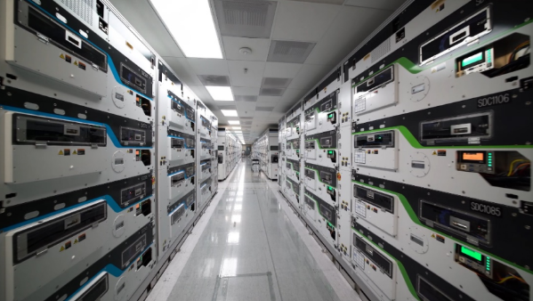
Figure. 1
In terms of manufacturing, Intel's Fab 52 in Arizona has successfully finished the Intel 18A run the lot, which signifies the first successful wafer trial at the facility and shows Intel's advancement in advanced process manufacturing. The Oregon fab will be the first to realize volume production of Intel 18A nodes, and manufacturing in Arizona is anticipated to enter the volume production ramp up later this year (ramp up). The ecosystem surrounding Intel Foundry is also improving, with reliable and established ecosystem partners offering a wide range of IP, EDA, and design services solutions to support Intel Foundry's expansion and propel technological advancement. With its initial focus on defining and advancing the role of advanced technologies in infrastructure development, the Intel Foundry Chiplet Alliance and the Value Chain Alliance are two new programs that have been added to the Accelerator Alliance of the Intel Foundry. The Intel Foundry Chiplet Alliance will give customers a dependable and scalable method to design products based on interoperable, secure chiplet solutions that meet specific application and market needs.


