

Should I lay copper under the inductor? PCB Design Guidelines for Low EMI DC/DC Converters
2024-11-28 11:45:10 1658
Every switching power supply is a broadband noise source. Therefore, integrating a DC/DC converter in an automotive circuit board network into an automotive control unit while still meeting the EMC requirements of the automotive original equipment manufacturer (OEM) can be a daunting task.
Typically, noise from DC/DC converters and other high-speed circuits radiates through the connected cables, which provide an effective antenna path for the noise. To block this potential radiation path, filter circuits are required at each cable connection point. However, filtering is only effective if the H-field or E-field of the noise source is not coupled into the filter assembly or cable.
In a near-field environment, the decrease in field strength is proportional to the inverse of the square of the distance (1/d2). Therefore, a certain minimum distance needs to be maintained between the noise source, the filter assembly and the connectors.
In practice, however, PCB dimensions and cable connector locations usually depend on the size of the mechanical space. Moreover, in some areas of the PCB, the maximum height of components may be very limited or double-sided assembly may not be possible. These hardware constraints require designers to be very careful when deciding on component placement and PCB layout, especially in highly regulated industries such as automotive manufacturing.
Layout Planning
To avoid the electric and magnetic fields of the DC/DC converter being directly coupled into connectors and cables, the circuitry must be located as far away as possible from the PCB connection points (see Figure 1).
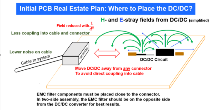
Figure 1: Noise sources should be located as far away as possible from connectors and cables
Only distance or additional shielding can reduce the field strength of EMC filters, connectors and cables to the necessary level, and shielding can replace distance.
The best way to do this is to use a PCB with at least 4 layers, assembled on both sides, and to place the DC/DC circuits and filter assemblies on opposite sides of the board. Also, at least one of the internal board layers is a complete grounding layer to minimize cross-coupling from the noise source to the filter circuitry.
If the DC/DC circuitry must be close to the connectors because of system limitations, effective shielding must be considered early in the design. Heat sinks can sometimes be used for shielding. Ideally, inductors, DC/DC ICs with built-in power MOSFETs, and their decoupling capacitors should be shielded.
PCB Layout Guidelines
In a buck converter, the main field sources include:
- A high di/dt loop (hot loop) formed by the two power switches and the CIN, which radiates a broadband magnetic field
- Open joints between power FETs and inductors that radiate strong electric fields
- Inductors that radiate electric and magnetic fields
AC magnetic fields can be shielded by solid metal regions capable of inducing eddy currents. Copper is a very effective shielding material due to its high conductivity. On a PCB, any conductor in a potential difference path that returns a fixed potential can be effectively shielded from electric field radiation.
Any high di/dt loop will radiate a magnetic field proportional to the loop area and current amplitude. The antenna loop area can be minimized by placing the input capacitors close to the two power switches and using a low impedance connection.
To further minimize the magnetic field generated by this loop, two sets of capacitors can be placed symmetrically at the power switches. Ideally, this will reduce the peak current in both loops by half, thereby reducing the H field by 6 dB. If the two loops are oriented in opposite directions, it will even further reduce the radiated H field. (1)
A complete GND area should be laid out on the next layer of the DC/DC circuit at a distance of less than 100 µm. In this copper-lined area, eddy currents are generated by the high di/dt currents flowing through the circuit components and PCB traces. The eddy currents are in the opposite direction to the original current on the component side and the two magnetic fields will cancel each other out. This works best if the eddy currents mirror the high di/dt loop current on the component side over the shortest distance.
In the ideal case of superconductivity, zero distance, and perfect matching of the two loop shapes, the H-field radiation on the component side of the PCB will be completely canceled by the H-field of the eddy current.
Because of the impedance in the copper-laid GND region below the DC/DC circuit, high di/dt eddy currents create a potential difference and make this region noisy. This noisy GND area must be separated from the system GND area, and in particular from any GND reference areas for filters and connectors. In a multilayer PCB, the layers can be laid out separately and isolated by through-hole impedance between the layers.
A three-dimensional view of a multilayer PCB illustrates this concept (see Figure 2).
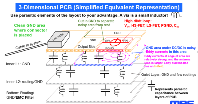
Figure 2: 3D PCB View - Layout is also part of the circuitry
On the top layer, the input capacitance (CIN) and the two power FETs are connected to the VIN area and the PGND area (as shown in red in the figure above), which are connected to the inner layer via via holes. On the VIN path, inductive components (e.g. 1µH to 2µH coils) have to be connected after the via holes. In this way, the high di/dt currents from the switching transitions will be confined in the CIN and will not flow on the PCB.
The PGND area should not be connected directly to any other GND on the component side, but only to the PGND area under the DC/DC module through a through-hole (as shown in blue in the figure above). The purpose of this is to limit high frequency currents to the component side and isolate noise from the “outside world”. at least one full layer of GND should be designed into the PCB to provide a low impedance system reference. Remember that layout is part of the circuit.
Should I lay copper underneath the inductors?
Some PCB layout tools are preset to not allow copper under the inductor core. Opinions vary on this issue, with some believing that no copper is needed at all, while others believe that copper should be placed directly under the coil on the component side of the PCB.
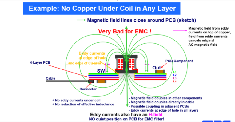
Figure 3: 4-Layer PCB without Copper Layer under the Coil
In the 4-layer PCB shown in Figure 3, no copper is laid in any of the layers below the coil, which generates the magnetic field shown in the figure. The strong magnetic lines of force generated by the coil go right to the bottom of the PCB and wrap around the PCB, effectively coupling it to any connected cables, while the filter assembly on the PCB is bypassed by air. With this design, it is virtually impossible to meet automotive OEM EMC standards.
Figure 4 shows a layout where the copper layer is laid directly under the coil on the component side.
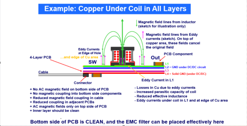
Figure 4: Copper layer directly below the coil on the PCB
This design provides an area for eddy currents to counteract the magnetic fields already present on the outside of the PCB. The inner layer 2 and the bottom layer are completely noise free. the EMC filter assembly can be effectively placed on the bottom. The eddy current field slightly reduces the effective inductance of the coil (typically less than 5%). Eddy currents also create some losses in the GND copper layer. Another small disadvantage of having the copper layer directly below the inductor core is that it increases the parasitic capacitance from the winding to GND. However, in most designs, this capacitance is so low that it does not make a big difference.
PCB Layout Example: MPQ443x Series
The MPQ443x Series are 40V synchronous buck converters with low operating quiescent current and 1A to 3.5A output current.
The MPQ4430 IC (U1) PCB has symmetrical CIN groups (C1A-C1D) on the top. The GND of these capacitors is directly connected to the IC PGND pin, the source of the bottom FET. This local GND area is noisy. On the component side, this GND area does not have a direct connection to any other GND area, and the only connection is through a vias to the GND area in the layer below the DC/DC circuit. In this configuration, the high di/dt current from the power stage is limited to the component side. The highest current density is located at the inner edge of the alignment between VIN and PGND, as shown by the green oval in the example (see Figure 5).
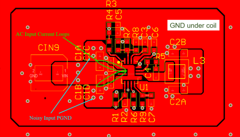
Figure 5: MPQ4430 PCB Top Layout
VIN is connected to Layer 3 through a via hole. The high frequency portion of the input current remains at the top due to the inductance of the vias. CIN9 suppresses this VIN node on the IC; however, it also blocks some of the E-field radiation from the SW node and the coil due to its 6mm height and cathode connection to GND.
The cutout around the top DC/DC module retains all high-frequency currents in that area. Without the cutout, a small portion of the hot loop current would still flow around the corners of the PCB, making that area noisy.
High dV/dt SW nodes are connected to inductors, which are usually large and radiate an electric field. For most inductors, the E-field radiation will be lower if the start of the winding is connected to the SW node.
One way to reduce the electric field radiation from a coil is to place output capacitors (C2A and C2B) on both sides of the coil. This works best when the capacitors are as tall or taller than the coil. In general, smaller, flatter inductors have better EMC performance than larger, taller coils.
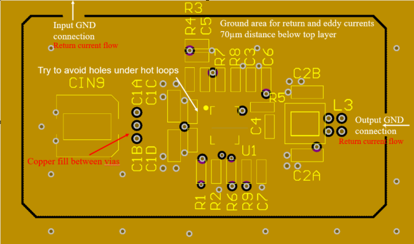
Figure 6: Recommended PCB layout for inner layer 1
The inner layer 1 of an EMC optimized PCB is the GND layer. This layer should be placed 70µm below the top (see Figure 6). This GND area is very noisy. A notch in the GND area around the DC/DC module prevents residual current from flowing around the edges of the layer below the connector and filter assembly. The notch should be two narrow openings exactly where VIN and VOUT are routed to the lower DC/DC circuit to provide a preset local return path. Test Results: 30MHz to 100MHz Conducted Emission
At fSW = 470kHz with Spectrum Spreading FM (SSFM), the conducted emissions from 30MHz to 108MHz were tested at approximately 0dBµV, which is only a few dB above the system noise (see Figure 7).
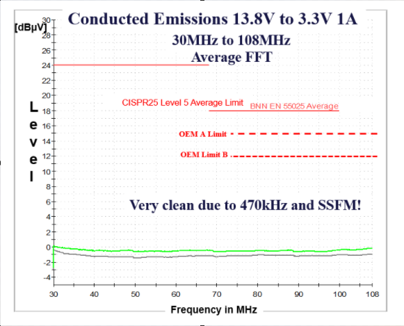
Figure 7: CE Emission Test Results (30MHz to 108MHz)
The MPQ4431 with 0805 2.2µH inductors and two 0805 output capacitors, and a switching frequency of 470kHz, also passes the low-frequency RE unipolar test without additional shielding or SSFM (see Figure 8).
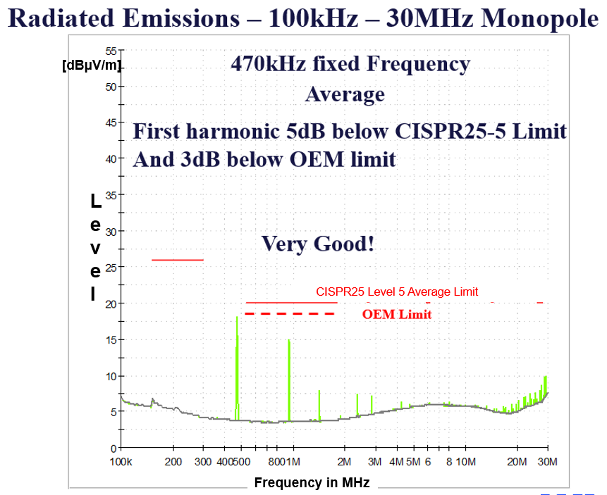
Figure 8: Low Frequency Unipolar Test Results
Conclusion
The layout and its parasitic components are also an integral part of the circuit. PCB optimization can achieve low EMI in DC/DC converters, and careful component placement and board layout will help meet the stringent EMC specifications of the automotive industry.


