

What is a charge pump? How does a charge pump work?
2025-01-22 15:55:49 767
A charge pump is a DC-DC converter that utilizes a capacitor as the energy storage element and is mostly used to produce an output voltage that is larger than the input voltage or to produce a negative output voltage. The electrical efficiency of a charge pump circuit is very high, about 90-95%, and the circuit is fairly simple. Charge pumps utilize a number of switching elements to control the voltage connected to the capacitor. This can be used, for example, in conjunction with a two-stage cycle where a lower input voltage is used to produce a higher pulse voltage output. In the first stage of the cycle, the capacitor is connected to the power supply terminal and is therefore charged to the same voltage as the power supply, and in the first stage the circuit configuration is adjusted so that the capacitor is in series with the supply voltage. If the effect of leakage current is not taken into account, and assuming no load, the output voltage will be twice the input voltage (the original supply voltage plus the voltage across the capacitor). The pulsed character of the higher output voltage can be filtered with the output filter capacitor.
Charge pump circuits are circuits that utilize switched-capacitor technology to achieve voltage conversion, primarily by alternately charging and discharging a capacitor to multiply or transform the voltage. Specifically, a charge pump circuit controls the charging and discharging process of a capacitor through carefully timed switching operations to convert an input voltage to a desired output voltage. Such circuits usually consist of a capacitor and a switch (e.g., a field-effect transistor) that operates by utilizing the charge-transfer characteristic of the capacitor. 1 Principle of operation
The principle of operation of a charge pump circuit is based on the property that the voltage of a capacitor cannot be changed instantaneously. When the switch is open, the capacitor is charged by an external power supply; when the switch is closed, the capacitor is discharged by an internal circuit to transfer the stored charge to the load. By continually cycling this process, the charge pump can multiply or transform the voltage.
How does a charge pump work?
The best way to understand this is to imagine the following scenario.
You charge a capacitor with a 9V battery, so the voltage across the capacitor is also 9 V. You then take another capacitor and charge it to 9 V. Now connect the two capacitors in series and measure the voltage across them - 18 V. This is the basic operation of a charge pump.
This is the basic principle of how a charge pump works - take two capacitors, charge them separately, and then connect them in series, although in a real charge pump the rearrangement is done electronically.
Of course, this is not limited to two capacitors; successive stages can be cascaded to obtain higher output voltages.
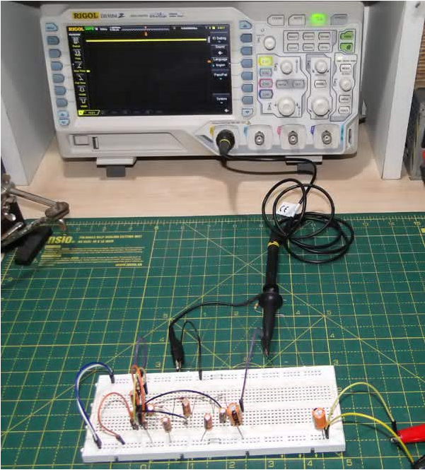
Figure. 1
Limitations of Charge Pumps
Before we build one, it is a good idea to understand the limitations of charge pumps.
1. available output current - since a charge pump is nothing more than a capacitor that charges and discharges cyclically, the available current is very low - in rare cases, 100mA can be obtained with the right chip, but the efficiency is very low.
2. the more stages you add does not mean that the voltage output increases that many times - each stage loads the output of the previous stage, so the output is not a perfect multiple of the input. The more stages you add, the worse this problem becomes.
Building a charge pump circuit
The circuit shown here is a simple three-stage charge pump using an Evergreen 555 timer IC. The circuit is “modular” in a sense - stages can be cascaded to increase the output voltage (given the second limitation).
Required Components
1. For 555 Oscillator
555 Timer - Bipolar
10uF electrolytic capacitor (decoupled)
2x 100nF ceramic capacitors (decoupled)
100pF Ceramic Capacitor (Timing)
1K Resistor (Timing)
10K Resistor (Timing)
2. For charge pump
6x IN4148 diodes (UF4007 is also recommended)
5x 10uF electrolytic capacitors
100uF electrolytic capacitor
An important point to note is that all capacitors used in the charge pump must be rated at a few volts higher than the expected output voltage.
Circuit Schematic
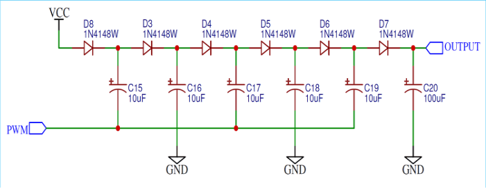
Figure. 2
This is what it looks like on a breadboard:
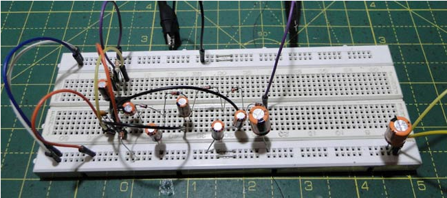
Figure. 3
Description of the charge pump circuit
1. 555 Timer
The circuit shown here is a simple 555 timer unregulated oscillator. The timing assembly generates a frequency of about 500kHz (a feat in itself for a bipolar 555). This high frequency ensures that the capacitors on the charge pump are “refreshed” periodically so that the output voltage does not ripple too much.
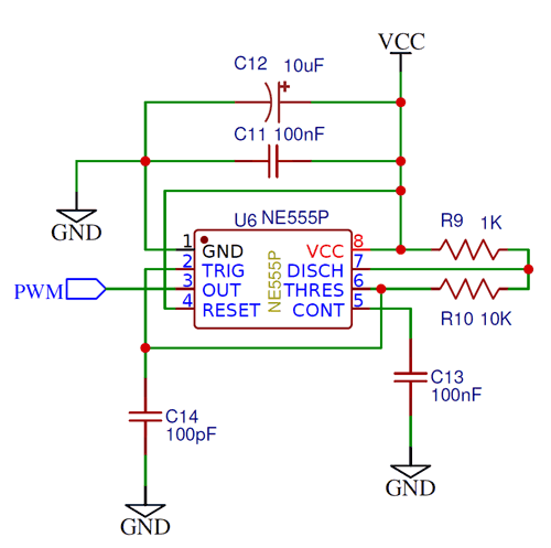
Figure. 4
Application Scenarios
Charge pump circuits are used in many applications, including:
Integrated circuits: to provide the required high voltage power inside a chip.
Analog circuits: for high-voltage power supply in amplifiers, filters, and other modules.
Wireless communications: to provide high-power, high-voltage power supplies in systems such as RF modules, antenna drivers, etc.
Sensors and actuators: Provide the required high voltage drive signals.
Medical equipment: such as pacemakers, medical imaging systems, etc., used to provide a stable high-voltage power supply.
Aerospace: to provide stable, high voltage output in equipment such as satellites and aircraft.
Automotive electronics: to meet the demand for high voltage signals in devices such as on-board sensors and motor drives.
Energy management: used in solar panels, wind turbines and other systems.
Advantages and Disadvantages
Advantages include:
Small size: does not require the use of inductors and is therefore much smaller than switch-mode regulators.
High efficiency: charge pumps offer higher conversion efficiency and lower static power consumption than linear regulators.
Programmable control: by controlling the operating mode and frequency of the switching tubes, the output voltage and power can be dynamically adjusted as needed.
Disadvantages include:
Lower efficiency: typically lower than switching regulators and higher output ripple and noise.
Limited applicability: suitable for applications with low load currents and moderate input/output voltage differences.
Charge Pump Applications
Charge pump converters are commonly used in voltage doubling or inverting DC-DC conversions. Charge pump circuits use capacitors as the intermediary for energy storage and transfer, with the advancement of semiconductor processes, new charge pump circuits can be switched at frequencies up to 1 MHz. there are two basic circuit forms of charge pumps: voltage doubling and voltage inversion.
Charge pump circuits are mainly used for voltage inverters, that is, the input positive voltage, the output is negative voltage, electronic products, often need positive and negative power supply or several different voltages to supply power to the battery-powered portable products, increase the number of batteries, will inevitably affect the size and weight of the product. The use of voltage inversion circuit can be eliminated in portable products in a group of batteries. As the operating frequency of 2 ~ 3MHz, so the capacitance is small, can use multi-layer ceramic capacitors (small loss, low ESR), not only to improve efficiency and reduce noise, and reduce the space of the power supply.
Although there are a number of DC / DC converter can be composed of boost, buck circuit can also be composed of voltage inversion circuit, but the charge pump voltage inverter only need to connect two capacitors, the circuit is the simplest, the size is small, and the conversion efficiency is high, less power consumption, so it has gained an extremely wide range of applications.
At present, many integrated circuits use a single power supply to work, simplify the power supply, but there are still many circuits need positive and negative power supply to work. For example, D / A converter circuits, A/D converter circuits, V / F or F / V converter circuits, operational amplifier circuits, voltage comparator circuits and so on. Since INTERSIL developed ICL7660 voltage inverter IC, it is very simple to get negative power supply with it, and voltage inverter circuit with voltage regulator has been developed after 90's, which makes negative power supply performance more perfect. For battery-powered portable electronic products, the use of charge pump converter to obtain the negative power supply or voltage doubling power supply, not only to reduce the number of batteries, reduce the size and weight of the product, and in reducing energy consumption (prolonging the life of the battery) plays a great role. Today's charge pumps can output up to 250mA of current with an efficiency of 75% (average).
How Charge Pump Negative Voltage Circuits Work
A charge pump negative voltage circuit is a DC/DC converter that utilizes capacitor energy storage, also known as a switched capacitor voltage converter. It can raise or lower the input voltage or even generate a negative voltage by charging and transferring the capacitor.
In a charge pump negative voltage circuit, a high level of the PWM (Pulse Width Modulation) waveform corresponds to Q2 being on, while a low level of the PWM corresponds to Q1 being on.VG1 is a step signal, usually set as a square wave with a certain amplitude and frequency. When the PWM signal of VG1 is at a high level, the direction of the current is VG1→C1→D1→GND, at this time, the capacitor C1 is charged, and the potential difference between its two ends is formed as left positive and right negative, i.e., VH. When the PWM signal of VG1 is at a low level, the direction of the current becomes C2→D2→C1→VG1, and at this time, C1 is discharged, and at the same time, the charge is applied to C2. Due to the characteristics of the capacitor voltage can not be changed abruptly, when the left end of C1 becomes 0, the VF1 end will become -VH, ignoring the voltage drop of D2, VF2 naturally get a negative voltage output -VH, this negative voltage value is affected by the frequency and amplitude of VG1.
Application Scenarios of Charge Pump Negative Voltage Circuit
Charge pump negative voltage circuit has a wide range of applications in electronic equipment, for example:
LCD screen backlight drive: LCD screen backlight needs high voltage drive, charge pump negative voltage circuit can convert low voltage to high voltage to drive LCD screen backlight.
Electronic discharge lamp driver: electronic discharge lamps need high-voltage drive, charge pump negative voltage circuit can be converted from low voltage to high voltage, drive electronic discharge lamps.
Electronic clock driver: Electronic clock needs low voltage driver, charge pump negative voltage circuit can convert low voltage to high voltage to drive electronic clock.
Electronic game machine drive: electronic game machine needs high voltage drive, charge pump negative voltage circuit can convert low voltage to high voltage, drive electronic game machine.
In short, the charge pump negative voltage circuit has a wide range of applications in electronic equipment, low voltage can be converted to high voltage, drive a variety of electronic equipment.
Conclusion
Charge pump negative voltage circuit is a kind of DC/DC converter using capacitor energy storage, which can realize the input voltage increase or decrease, and even generate negative voltage. This article describes in detail the working principle and application scenarios of charge pump negative voltage circuit. In electronic equipment, charge pump negative voltage circuit has a wide range of applications, can be converted from low voltage to high voltage, drive a variety of electronic equipment.


