

Why did HMC lose out to HBM?
2025-06-10 14:50:09 1057
Both HMC (Hybrid Memory Cube) and HBM (High Bandwidth Memory) were developed with the goal of replacing DDRx. They share similar names, structures, and both utilize 3D TSV technology, with performance levels surpassing that of DDRx by several times during the same period.
Driven by the AI boom, HBM has reached its peak, while HMC has quietly faded into the background. What factors led to such a significant disparity? This article will analyze the underlying reasons.
HMC
HMC (Hybrid Memory Cube) was once hailed as a revolutionary technology with great expectations.
Developed by Micron and Intel, HMC was initially designed to address the bandwidth limitations of DDR3.
Launched in 2011, HMC held significant strategic importance for Micron, as it was seen as a key weapon to compete against South Korean giants Samsung and SK Hynix.
In the HMC standard, four DRAM dies are connected via 3D TSV to the logic control chip (Logic Die) at the bottom of the stack. The schematic diagram is shown below:
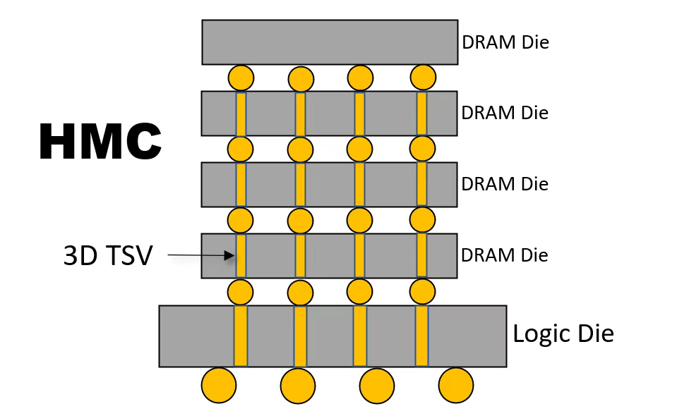
Figure 1
TSV technology was first developed in 1999 and was the first to be commercially applied in the memory industry. It is the most important technology in the field of advanced packaging, without a doubt.
In 2011, HMC leveraged the momentum of TSV technology to win the “Best New Technology Award” in that year's “Microprocessor Report,” gaining widespread attention.
In HMC design, communication between the CPU processor and the memory stack is conducted via a high-speed SERDES data link, which connects to the logic controller chip at the bottom of the DRAM stack. The processor is not integrated into the stack, thereby avoiding issues such as mismatched chip sizes and thermal management. However, this approach introduces a new challenge: the processor is relatively distant from the memory stack, which would later become a significant drawback for HMC.
An HMC is essentially a complete DRAM module that can be installed on a multi-chip module (MCM) or a 2.5D passive connector to bring it closer to the CPU, though no one actually does this.
Additionally, Micron has introduced a “remote memory” configuration where part of the HMC is connected to the host, while another part of the HMC is connected to other HMCS via serial links to form a memory cube network.
Regarding the latency concerns many have raised, Micron states that while the serial links in HMC may slightly increase system latency, overall latency is significantly reduced. HMC achieves approximately three times the energy efficiency of DDR4 (measured in pj/bit).
HBM
HBM (High Bandwidth Memory) is a high-bandwidth memory solution that stacks multiple DRAM chips together and integrates them with a GPU, creating a high-capacity, high-bandwidth DRAM array.
First, HBM vertically stacks memory chips, with four DRAM dies connected to the logic control chip (Logic Die) at the bottom of the stack via 3D TSVs, which is similar to HMC. Then, these DRAM stacks are connected to the CPU or GPU via an interposer layer.
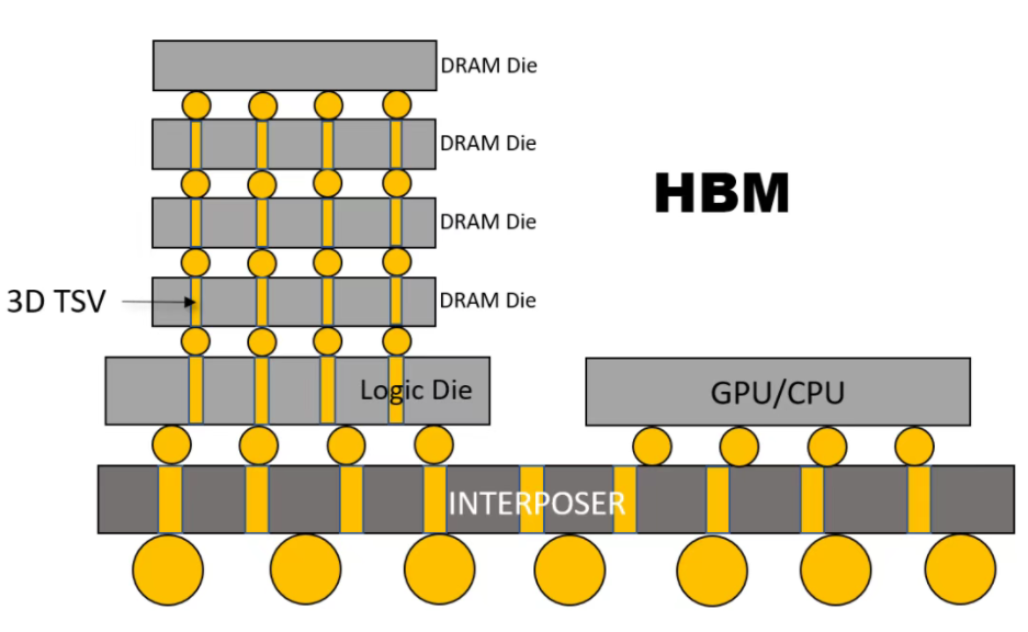
Figure 2
Although these HBM stacks are not 3D-integrated with the CPU or GPU, they are tightly and quickly connected via the interposer layer, making HBM's characteristics nearly indistinguishable from on-chip integrated RAM.
HBM was co-developed by Hynix and AMD, with its launch in 2013, two years after HMC.
HBM uses a 128-bit wide channel, with up to 8 channels stackable to form a 1024-bit interface, offering a total bandwidth ranging from 128GB/s to 256GB/s.
HMC vs HBM
Comparing HMC and HBM, we can see how similar they are: both stack DRAM on top of a logic controller, both use 3D TSV technology, and both were developed by major manufacturers (HMC: Micron + Intel; HBM: Hynix + AMD). HMC was launched in 2011, and HBM in 2013, which is also quite close.
Today, HBM is thriving, while HMC has faded from the scene. What are the reasons behind this?
I believe there are two main factors: 1. Structural differences, 2. Industry standards.
Structural differences:
Although HMC and HBM share similar structures—both stack DRAM on top of a logic controller and utilize 3D TSV technology—HBM incorporates an additional interposer layer. This interposer tightly integrates the DRAM stack with the GPU. In essence, wherever there is a GPU, there is HBM.
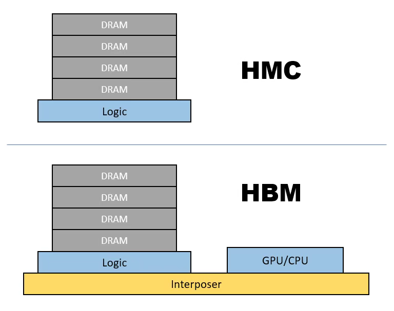
Figure 3
HBM has established its position through GPUs, with both AMD and NVIDIA choosing HBM as the memory for their graphics cards, coinciding with the AI boom, making it hard not to be popular.
HMC's method of placing the memory stack far from the CPU/GPU means that most of the advantages of 3D chip stacking and inherent low latency are lost, as the laws of physics cannot be escaped, and signal transmission speeds are limited. Distance translates to greater latency.
Assuming systems containing HBM and HMC respectively, we can plot the smallest cube and examine its functional density—the number of functional units per unit volume, which can be simply understood as the number of transistors per unit volume. It is evident that HBM is significantly larger than HMC, meaning HBM has higher functional density. Therefore, as a key metric for advanced packaging, HBM is more advanced.
Under the premise that heat can be dissipated, the design principle of advanced packaging is to be as compact as possible. For this reason, I proposed the functional density law as an important basis for describing system integration.
Through 3D TSV integration and vertical stacking of chips, an important issue regarding the distance between transistors and other microcomponents on the chip is resolved. By vertically stacking devices together, the distance between them can be minimized, thereby reducing latency and power consumption. Both HMC and HBM achieve this.
However, HMC lacks an interposer, preventing it from tightly integrating with CPUs/GPUs, thereby affecting its functional density. In contrast, HBM uses an interposer to tightly integrate memory stacks with CPUs/GPUs, effectively enhancing its functional density and gaining a competitive edge.
HMC is a typical 3D integration technology, while HBM is a step above, referred to as 3.5D integration technology. Don't underestimate this 0.5-dimensional difference—it enables tighter integration, thereby increasing the system's functional density.
From a structural perspective, what is the true reason HBM outperforms HMC? Distance.
Some ask, is HMC outperformed by HBM because it is 3D packaging while HBM is 3.5D? Yes, that is indeed one way to interpret it.
Industry standards:
The structural shortcomings of HMC inevitably make it inferior to HBM in terms of functional density. After HBM was introduced, HMC's decline became evident. The fatal blow to HMC was that shortly after HBM was introduced, it was established as the JEDEC industry standard, while HMC, despite being introduced two years earlier, was only supported by a single HMCC.
One is a major organization recognized by most tech companies in the industry, while the other is a small circle initiated by Micron. The outcome was already decided before the competition even began.
JEDEC, with hundreds of member companies, follows a one-company-one-vote system with a two-thirds majority requirement, thereby reducing the risk of any single company or group of companies controlling the standard-setting process. In other words, the authority over JEDEC standards is not held by industry giants; only standards that are truly recognized by all parties will ultimately be adopted as official standards.
In 2018, as artificial intelligence began to gain traction, high bandwidth became the focal point of the memory industry. HBM, closely tied to GPUs, secured the largest market share, with Hynix and Samsung, the main promoters of the standard, emerging as the big winners. HBM's major clients, NVIDIA and AMD, also reaped substantial profits as a result.
HMC has long since lost the glory it had when it was first launched in 2011, with few takers. Micron no longer clings to it and officially abandoned HMC in August 2018, shifting to HBM.
Micron was simply too late to the game, and its market share lags significantly behind the two Korean manufacturers. According to the latest data, SK Hynix holds a 50% share of the global HBM market, ranking first; Samsung follows closely behind with a 40% share; and Micron trails in third place with just a 10% market share.
The rise of artificial intelligence may have been the final straw that broke the camel's back for HMC.
At this point, Micron can't help but sigh: Why were both Yu and Liang born?
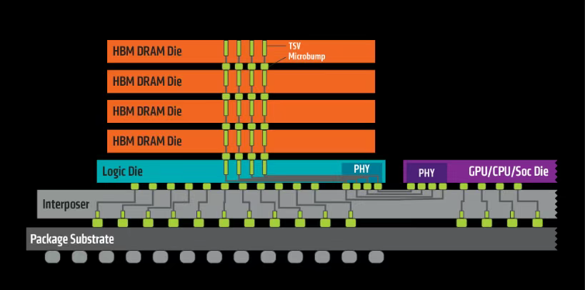
Figure 4
In the semiconductor industry, new technologies emerge constantly, like ripples on a lake, sparkling with the brilliance of science and technology. Some technologies once shone brightly but eventually faded away, while others have stood the test of time and driven great advancements in human technology. The victors are celebrated, while the defeated are forgotten—the semiconductor industry is no exception.


