

5CEFA5U19I7N FPGAs: Features, Applications and Datasheet
2025-01-20 10:30:54 847
5CEFA5U19I7N Description
The 5CEFA5U19I7N is an FPGA from the Intel Cyclone V family, designed to offer low power consumption and high performance for mid-range applications. It features an extensive array of logic elements, embedded memory, and programmable I/O pins, providing an ideal solution for applications requiring efficient digital signal processing, embedded systems, and flexible I/O configurations. The device is available in a 19x19 mm UFBGA package with 484 pins, allowing for high-density and compact designs.
5CEFA5U19I7N Features
Logic Elements: 49,760 logic elements for handling complex designs.
Embedded Memory: 3,383 Kbits of embedded memory blocks for fast data access.
Transceivers: Integrated transceivers for high-speed serial data transmission (up to 6.6 Gbps).
I/O Pins: Supports up to 290 user I/O pins for flexible interfacing.
Clock Management: Built-in clock management resources including PLLs for precise timing control.
Low Power Consumption: Optimized for low-power operation, making it suitable for battery-powered applications.
Temperature Range: Operates in an industrial temperature range from -40°C to 100°C.
Package Type: Available in a 484-pin UFBGA package for high-density applications.
5CEFA5U19I7N Applications
Industrial Automation: Used in industrial control systems, machine vision, and robotics for automation tasks.
Telecommunications: Suitable for communication infrastructure, including data transmission, routing, and switching applications.
Automotive: Ideal for in-vehicle communication and processing systems, such as ADAS (Advanced Driver Assistance Systems).
Embedded Systems: Applied in embedded devices requiring high flexibility and real-time processing.
Consumer Electronics: Utilized in consumer electronics like digital TVs, home entertainment systems, and smart home devices.
Data Centers: Suitable for processing data in high-throughput applications and managing power in energy-efficient systems.
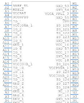
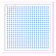
5CEFA5U19I7N CAD Model
Symbol
Footprint
3D Model


5CEFA5U19I7N Alternatives
Xilinx Artix-7 Series: Offers similar performance and power efficiency for mid-range FPGA designs.
Lattice ECP5: Another alternative with low-power consumption and high-speed transceiver support for embedded designs.
Intel Cyclone IV: A lower-density alternative from Intel for less complex designs with similar power and I/O capabilities.
Microsemi SmartFusion2: Provides mixed-signal FPGAs with programmable logic and ARM-based processors for embedded applications.
Altera MAX 10: Offers a cost-effective solution for smaller designs requiring fewer logic elements and simpler I/O configurations.
5CEFA5U19I7N FAQs
What is the maximum clock frequency for the 5CEFA5U19I7N?
The 5CEFA5U19I7N supports clock frequencies of up to 300 MHz, depending on the design and specific configuration.
What programming tools are compatible with the 5CEFA5U19I7N?
It is supported by Intel’s Quartus Prime software for design, simulation, and programming, along with the use of JTAG for in-system configuration.
Does the 5CEFA5U19I7N support high-speed serial interfaces?
Yes, it integrates transceivers that support speeds up to 6.6 Gbps for high-speed serial communication.
What is the power consumption of the 5CEFA5U19I7N in typical applications?
Power consumption varies based on the application and configuration, but it is optimized for low-power operation, typically drawing between 1W to 10W, depending on logic utilization.
What is the I/O voltage range supported by the 5CEFA5U19I7N?
The 5CEFA5U19I7N supports I/O voltage levels ranging from 1.2V to 3.3V, allowing for flexible interfacing with different external components.


