

EP3C16F484C8N Intel FPGAs: Features, Applications and Datasheet
2025-07-02 10:00:42 635
EP3C16F484C8N Description
The EP3C16F484C8N is a mid-density FPGA from Intel’s Cyclone III family, offering 15,408 logic elements, optimized for low power and cost-sensitive applications. Packaged in a 484-pin FBGA, it supports a wide range of I/O standards and is suitable for embedded, control, and signal-processing systems.
EP3C16F484C8N Features
15,408 logic elements (LEs)
504 Kbits of embedded SRAM
56 embedded 18x18 multipliers for DSP functions
Up to 331 user I/O pins
Four integrated PLLs for flexible clock generation
Supports Passive Serial, Active Serial, and JTAG configuration modes
1.2V core voltage; supports multiple I/O voltages (1.8V, 2.5V, 3.3V)
Low static and dynamic power consumption
Compatible with various I/O standards, including LVDS, SSTL, HSTL
EP3C16F484C8N Applications
Industrial automation controllers
Embedded image and video processing systems
Communication interface bridging (e.g., SPI to UART)
Renewable energy system controllers
Medical device logic control
Educational FPGA platforms
I/O expansion boards and custom SoC prototypes
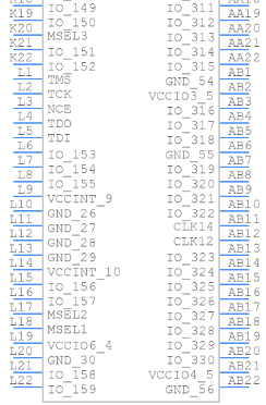
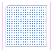
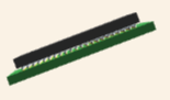
EP3C16F484C8N CAD Model
Symbol
Footprint
3D Model

EP3C16F484C8N Alternatives
EP3C25F484C8N: Same package with higher logic capacity (24,624 LEs)
EP3C10F484C8N: Same package with fewer resources (10,320 LEs)
EP4CE15F23C8N: Cyclone IV E successor with better power efficiency
EP3C16F256C8N: Same logic size in smaller 256-pin package
EP2C20F484C8N: Older Cyclone II FPGA, same package, fewer features
EP3C16F484C8N Manufacturer
Intel Corporation is a global leader in semiconductor innovation, best known for designing and manufacturing advanced microprocessors and related technologies that power the majority of the world’s computers and connected devices. Founded in 1968 and headquartered in Santa Clara, California, Intel pioneered the x86 architecture, which has become the foundation of most modern personal computers.
Over the decades, Intel has expanded its portfolio beyond CPUs to include FPGAs, system-on-chip (SoC) solutions, graphics processing units (GPUs), networking hardware, AI accelerators, and memory technologies. The company serves diverse industries such as cloud computing, artificial intelligence, autonomous driving, communications, and edge computing.
With a strong focus on innovation, Intel continues to drive technological advancement through cutting-edge manufacturing processes, including its transition to Intel 7, Intel 4, and future nodes. As a trusted technology provider, Intel plays a key role in shaping the future of computing and digital transformation globally.
EP3C16F484C8N FAQs
What kind of clock sources can be used with EP3C16F484C8N?
The device can accept external clock inputs through dedicated global clock pins and can generate derived clocks using its internal PLLs.
How is power distributed internally within the EP3C16F484C8N?
The FPGA uses separate power rails for the core (1.2V), I/O banks (1.8V/2.5V/3.3V), and auxiliary circuits, enabling flexible system-level power design.
Is partial reconfiguration supported on this device?
No, Cyclone III FPGAs do not support partial reconfiguration; the entire configuration memory must be updated as a whole during reprogramming.
Can EP3C16F484C8N interface directly with external flash memory?
Yes, it can interface with serial flash memory (such as EPCS devices) for Active Serial configuration and can also communicate with parallel flash via user logic.
What are the static power characteristics of the EP3C16F484C8N?
Thanks to its 65nm low-power process, the device consumes less than 0.5W in most standby or low-activity use cases, depending on configuration and I/O activity.


