

Several ways to control EMI radiation using PCB layered stacking
2024-12-20 11:14:42 779
There are many ways to solve the EMI problem, modern EMI suppression methods include: the use of EMI suppression coating, selection of appropriate EMI suppression spare parts and EMI simulation design. In this paper, from the most basic PCB board, discuss the role of PCB layered stacking in the control of EMI radiation and design techniques.
Power supply busbar
Proper placement of capacitors of appropriate capacity near the power supply pins of an IC can make the jump in the output voltage of the IC come faster. However, the problem does not end there. Due to their finite frequency response, capacitors are unable to generate the harmonic power needed to cleanly drive the IC's output over the full frequency band. In addition to this, the transient voltages developed on the power bus form voltage drops across the inductors in the decoupling path, and these transients are the main source of common-mode EMI interference. How should we solve these problems?
In the case of our ICs on the board, the power supply layer around the IC can be thought of as a good high-frequency capacitor, which collects the portion of energy leaked from the discrete capacitors that provide high-frequency energy for the clean output. In addition, a good power supply layer has a small inductance so that the transient signals synthesized by the inductor are small, thus reducing common mode EMI.
Of course, the power supply layer to the IC power pins must be as short as possible, because the rising edge of the digital signal is getting faster and faster, it is best to connect directly to the IC power pins where the pads are located, which is to be discussed separately.
In order to control common mode EMI, the power supply layer should help decoupling and have a low enough inductance, this power supply layer must be a pair of power supply layers that are fairly well designed. One might ask, how good is good enough? The answer to this question depends on the layering of the power supply, the materials between the layers, and the operating frequency (i.e., a function of the IC's rise time). Typically, with a power supply layered at 6 mil spacing and FR4 interlayers, the equivalent capacitance of a power supply layer per square inch is about 75 pF. Obviously, the smaller the layer spacing, the higher the capacitance.
There are not many devices with a rise time of 100 to 300ps, but according to the current development speed of ICs, devices with a rise time in the range of 100 to 300ps will occupy a high proportion. For circuits with a rise time of 100 to 300 ps, the 3 mil layer pitch will no longer be suitable for most applications. At that time, it is necessary to use layer spacing less than 1 mil of layering technology, and with a high dielectric constant material instead of FR4 dielectric materials. Today, ceramics and vitrified plastics can meet the design requirements of 100 to 300 ps rise time circuits.
Although new materials and methods may be used in the future, for today's common 1 to 3ns rise time circuits, 3 to 6 mil layer spacing and FR4 dielectric materials are usually sufficient to deal with the high end harmonics and make the transient signals low enough, that is to say, common-mode EMI can be reduced to a very low level. The PCB layered stacking design examples given in this article will assume a layer spacing of 3 to 6 mil.
Electromagnetic Shielding
In terms of signal alignment, a good layering strategy would be to place all signal alignments in one or more layers that are immediately adjacent to the power or ground layers. For power supplies, a good layering strategy would be to have the power and ground layers next to each other, and the distance between the power and ground layers should be as small as possible, which is what we call a “layering” strategy.
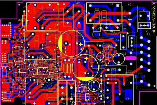
Figure. 1
PCB Stacking
What kind of stacking strategy helps to shield and suppress EMI? The following layered stacking scheme assumes that power currents flow on a single layer, and that single or multiple voltages are distributed on different parts of the same layer. The case of multiple power supply layers will be discussed later.
4-Layer Boards
There are several potential problems with 4-layer board designs. First, a traditional four-layer board with a thickness of 62 mil has too much spacing between the power and ground layers, even though the signal layer is on the outer layer and the power and ground layers are on the inner layer.
If cost requirements are paramount, consider the following two alternatives to the traditional 4-layer board. Both programs can improve the performance of EMI suppression, but only applies to the board component density is low enough and enough area around the components (placed in the required power supply copper cladding) of the occasion.
The first is the preferred option, the outer layer of the PCB are ground layer, the middle two layers are signal / power layer. The power supply on the signal layer is routed with a wide line, which allows for a low path impedance for the power supply current and a low impedance for the signal microstrip path. From an EMI control perspective, this is the best available 4-layer PCB structure. The second option has an outer layer going to power and ground, and two middle layers going to signal. This scheme is less improved compared to the traditional 4-layer board, and the interlayer impedance is as poor as the traditional 4-layer board.
If alignment impedance is to be controlled, all of the above stacking schemes have to be very careful to arrange the alignments underneath the power and ground laying copper islands. In addition, the copper-laying islands on the power or ground layers should be interconnected as close as possible to each other to ensure DC and low-frequency connectivity.
6-Layer Boards
If the component density on a 4-layer board is relatively high, a 6-layer board is preferred. However, certain stacking schemes in 6-layer board designs do not provide good enough shielding against electromagnetic fields and provide little reduction of power sink transients. Two examples are discussed below.
The first example places the power supply and ground in layers 2 and 5, respectively, which is very detrimental to controlling common mode EMI radiation due to the high power supply copper cladding impedance. However, from the signal impedance control point of view, this method is very correct.
The second example of the power supply and ground are placed in the 3rd and 4th layers, this design solves the problem of power supply copper-clad impedance, due to the poor electromagnetic shielding performance of the 1st and 6th layers, the differential mode EMI increased. If the number of signal lines on the two outer layers is minimal and the alignment length is very short (shorter than 1/20 of the signal's highest harmonic wavelength), this design solves the differential mode EMI problem. The outer layer of the component-free and non-aligned areas of copper-filled and grounded copper-clad areas (every 1/20 wavelength interval), the differential mode EMI suppression is particularly good. As mentioned earlier, connect the copper-layered areas to the internal grounding layer at multiple points.
General-purpose high-performance 6-layer board design will generally be the first and sixth layer cloth for the ground layer, the third and fourth layer to go power and ground. EMI rejection is excellent due to the two centered dual microstrip signal line layers between the power and ground layers. The disadvantage of this design is that there are only two alignment layers. As described earlier, the same stack can be realized with a conventional 6-layer board if the outer layer is short and copper is laid in the non-aligned area.
An alternative 6-layer board layout is Signal, Ground, Signal, Power, Ground, Signal, which enables the environment required for advanced signal integrity designs. The signal layer is adjacent to the ground layer, and the power and ground layers are paired. Obviously, the downside is the unbalanced stacking of the layers.
This usually causes problems in processing and manufacturing. The solution to this problem is to fill all the blank areas of layer 3 with copper. If the density of the copper cladding on layer 3 is close to that of the power or ground layers, the board can be considered not strictly structurally balanced. The copper-filled areas must be connected to power or ground. The distance between the connection holes is still 1/20th of a wavelength, not necessarily everywhere, but ideally they should be.
10-layer boards
Because of the very thin insulating barrier between layers, the impedance between layers of a 10- or 12-layer board is very low, and excellent signal integrity can be expected as long as delamination and stacking are not a problem. It is more difficult to process and manufacture 12-layer boards at 62 mil thickness, and not many manufacturers are able to process 12-layer boards.
Since there is always an insulating layer between the signal layer and the loop layer, it is not optimal to allocate the middle 6 layers in a 10-layer board design to route the signal lines. Also, it is important to have the signal layer adjacent to the loop layer, i.e., the board layout is signal, ground, signal, signal, power, ground, signal, signal, ground, signal.
This design provides good pathways for signal currents and their loop currents. The proper wiring strategy is to route layer 1 in the X direction, layer 3 in the Y direction, layer 4 in the X direction, and so on. Intuitively looking at the alignment, Layer 1 1 and Layer 3 are a pair of layered combinations, Layer 4 and Layer 7 are a pair of layered combinations, and Layer 8 and Layer 10 are the last pair of layered combinations. When it is necessary to change the direction of the line, the signal line on layer 1 should be “perforated” to layer 3 before changing direction. In practice, this may not always be possible, but as a design concept it should be adhered to as much as possible.
Similarly, when signals change direction, they should be routed through vias from layers 8 and 10 or from layer 4 to layer 7. This routing ensures the tightest coupling between the signal's forward path and the loop. For example, if the signal is routed on Layer 1 and the loop is on Layer 2 and only on Layer 2, then even if the signal on Layer 1 is transferred to Layer 3 through a “via”, the loop will still be on Layer 2, thus maintaining low inductance, high capacitance, and good EMI shielding.
What if this is not the case? For example, if the signal line on layer 1 goes to layer 10 through a via, the loop signal has to find the ground plane from layer 9, and the loop current has to find the nearest grounded via (e.g., the ground pin of a component such as a resistor or capacitor). If such an aperture happens to exist nearby, you are in luck.
If there is no such close aperture available, the inductance will be larger, the capacitance will have to be reduced, and the EMI will definitely increase. When a signal line must leave the current pair of wiring layers via a vias to other wiring layers, a grounding vias should be placed close to the vias so that the loop signals can be smoothly returned to the proper grounding layer. For Layer 4 and Layer 7 layered combinations, the signal loop will return from either the power or ground layer (i.e., Layer 5 or Layer 6) because the capacitive coupling between the power and ground layers is good and the signal is easily transmitted.
Design of Multiple Power Supply Layers
If two power supply layers of the same voltage source are required to output large currents, the board should be laid out in two sets of power supply and ground layers. In this case, an insulating layer is placed between each pair of power and ground layers. This results in two pairs of power supply buses of equal impedance that we expect to divide the current equally. If the stacking of the power supply layers results in unequal impedances, the shunt will not be uniform, transient voltages will be much larger, and EMI will increase dramatically.
If there are multiple supply voltages with different values on the board, multiple power supply layers will be required accordingly, keeping in mind to create their own paired power and ground layers for the different power supplies. In both cases, keep in mind the manufacturer's requirements for a balanced structure when determining the location of the paired power and ground layers on the board.
Summarizing
Given that most engineers design boards that are 62 mil thick, conventional printed circuit boards without blind or buried vias, this article is limited to a discussion of board layering and stacking. For boards that vary greatly in thickness, the layering schemes recommended in this article may not be ideal. In addition, boards with blind or buried vias are processed differently and the layering methods in this article are not applicable.
Circuit board design in the thickness, through-hole process and the number of layers of the board is not the key to solving the problem, excellent layered stack is to ensure that the power bus bypass and decoupling, so that the power layer or ground layer to minimize transient voltages and will be shielded from the electromagnetic field of the signal and the power supply is the key to the key. Ideally, there should be an insulating barrier between the signal alignment layer and its loop ground layer, and the paired layer spacing (or more than one pair) should be as small as possible. Based on these basic concepts and principles, it is possible to design a board that always meets the design requirements. Now that IC rise times are short and will be shorter, the techniques discussed in this article are essential to solving EMI shielding problems.


