

Why are PCBs deformed? What are the hazards?
2025-04-01 17:21:06 1087
PCB deformation risks
Circuit boards that are not flat will result in incorrect placement in the automated surface mount line, make it impossible to mount or insert components into the board's holes and surface mount pads, and possibly even cause the automatic insertion machine to malfunction.
It is challenging to cut component feet neatly and flat once they have been welded into the circuit board. The assembly factory experienced board warping, which is also quite frustrating, because the board cannot be inserted into the chassis or machine socket.
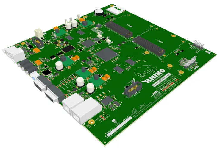
Figure. 1
As a home for a multitude of components, PCB boards have higher requirements, and contemporary surface mount technology is developing toward high precision, high speed, and intelligent direction.
According to the IPC standard, a PCB board for a surface-mount device may deform by 0.75 percent; however, no surface-mount PCB board permits deformation over 1.5 percent.
Actually, some electronic assembly manufacturers have stricter standards for deformation, such as a 0.5% allowable amount of distortion and even 0.3% individual requirements, in order to satisfy the demands of high precision and high speed installation.
Because the materials used to make PCB boards—copper foil, resin, glass cloth, and other materials—have different physical and chemical characteristics, pressing them together would unavoidably result in residual thermal stress and deformation.
At the same time, a number of processes, including high temperature, mechanical cutting, and wet processing, will also have a significant effect on the board's deformation. In other words, there are many different and complex reasons why PCB boards can deform, and one of the complicated issues that PCB manufacturers face is how to lessen or eliminate deformation caused by various material properties or processing-induced deformation.
Analysis of PCB board deformation
The article will be able to generate deformation of the different causes and improvement ways to study and elaborate. PCB board deformation must be investigated from the material, structure, graphic distribution, processing, and other aspects of the process.
Board warping and bending will be exacerbated by an uneven copper surface area.
Figure 2.
In general, circuit boards are made with a lot of copper foil for grounding, and occasionally, the Vcc layer is made with a lot of copper foil as well. Uneven heat absorption and dissipation will result from the uneven distribution of these sizable copper foil sections on the same board.
Naturally, the board will also undergo thermal expansion and contraction; if these processes cannot occur simultaneously, the board will experience distinct stress and deformation. Additionally, if the board's temperature reaches the upper limit of the Tg value, the board will start to soften, which will cause deformation.
The board's ability to expand and compress will be restricted by the vias and holes connecting each layer.
The majority of modern circuit boards are multilayer, with rivets holding the connection points (vias) between the layers. The connection points are separated into blind, buried, and through holes, and they will limit the impact of cold shrinkage on the board while also indirectly causing warping and bending.
Causes of PCB board deformation include:
(1) the circuit board's weight, which causes the board to sink and distort
As a fulcrum to support the entire board, the chain is used in a general soldering furnace to drive the circuit board forward, that is, to the board on both sides.
Board bending will result from the weight of the board itself exhibiting the phenomena of the center of the depression if there are excessively heavy components on the board or if the board is too big.
(2) The amount of board deformation will depend on the depth of the V-Cut and the connecting strip.
In essence, the V-Cut is the one responsible for destroying the board's structure because it is prone to deformation and is used to cut out grooves on the original sheet.
Impact of structure, graphics, and press-fit material on board deformation:
PCB board The degree of deformation caused by the pressing of heat deformation between the core board and copper foil is determined by the coefficient of thermal expansion (CTE) of the two materials. The core board and semi-cured sheet and the outer layer of copper foil are pressed together.
Copper foil has a coefficient of thermal expansion (CTE) of roughly 17X10-6, whereas the Z-direction CTE of a typical FR-4 substrate is (50~70)X10-6 below the Tg point and (250~350)X10-6 above the TG point. Because glass cloth is present, the X-direction CTE is often comparable to that of copper foil.
Deformation brought on by processing PCBs
The reasons of deformation in PCB board production are extremely complicated and can be separated into two categories: mechanical stress and thermal stress.
The press process is the primary source of thermal stress, whereas the handling, stacking, and baking of boards are the primary sources of mechanical stress. A basic explanation of the process order is given below.
1. Incoming copper-clad laminates: These laminates are all double-sided, symmetrical, and graphic-free. Additionally, because the CTE of copper foil and glass cloth is so comparable, there is seldom any distortion during the pressing process due to different CTE.

Figure. 3
However, due to the laminate press's size and the temperature differential between the hot plate's various sections, there will be minor variations in the degree and speed of curing of the resin in various areas during the lamination process. Additionally, the dynamic viscosity at various heating rates will also vary, resulting in local stresses brought on by variations in the curing process.
After pressing, this tension is typically kept balanced, although it will be progressively released throughout subsequent processing to cause deformation.
2. Pressing: The primary source of thermal stress is the PCB pressing process, and the pressing of copper-clad board, like the curing process, will result in variations in local stresses. Additionally, because PCB board has a thicker, more graphic distribution of semi-cured sheets, its thermal stresses will be higher than those of copper-clad board, which is more challenging to remove.
When the PCB board is under stress, it will flex as a result of further drilling, shaping, grilling, and other activities.
3. Soldermask, characters, and additional baking procedures: Since Soldermask ink cannot be stacked on top of one another, the PCB board will be positioned vertically in the shelf baking board curing. The soldermask temperature will be around 150 °C, slightly above the Tg point of the low Tg material and above the Tg point of the resin. The board is susceptible to deformation when subjected to self-weight or strong oven winds.
4. Hot air solder leveling: The oven is set to 225°C to 265°C and is run from 3 to 6 seconds. The hot air has a temperature between 280°C and 300°
Two minutes after the post-treatment washing and room temperature, solder the leveling board from room temperature into the tin furnace. the complete hot air solder leveling procedure for the abrupt temperature changes.
Thermal stresses will inevitably arise throughout the hot and cold process because of the circuit board's uneven structure and diverse materials, which will cause microscopic strains and general deformation warpage.
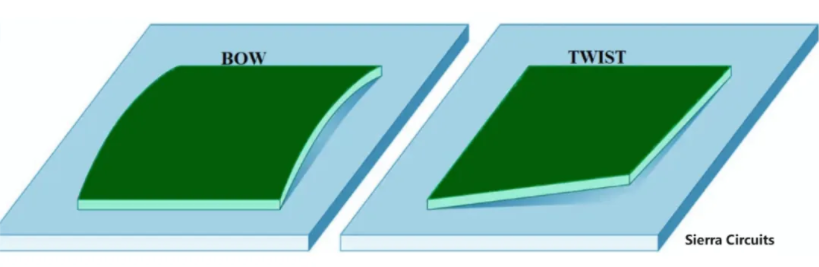
Figure 4.
5. Storage: When PCB boards are in the semi-finished stage of storage, they are typically placed vertically in the rack, the rack is not correctly set, or the stacking of boards during storage causes mechanical deformation of the board, among other issues. Particularly for the more severe impact that is 2.0 mm below the thin board.
The deformation of the PCB board is influenced by numerous additional elements in addition to the ones mentioned above.
Preventing PCB bending and deformation
PCB warpage has a significant effect on printed circuit board production. It is also a significant problem in the circuit board manufacturing process, since component feet are challenging to neaten and laden with bending board components after soldering.
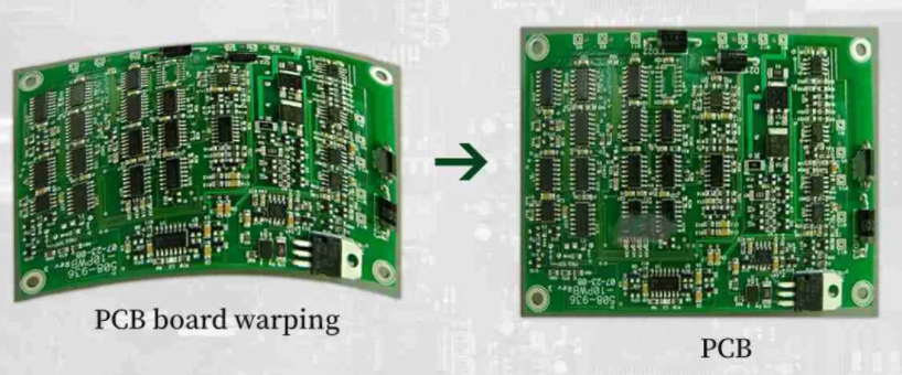
Figure 5
Additionally, the board cannot be mounted to the machine's chassis or sockets, so board warpage interferes with the post-process's ability to function normally. The manufacturing requirements for board warpage are increasing as printed circuit boards move into the era of surface mount and chip mount.Therefore, we must identify the source of circuit board warpage.
1. Design of engineering: Precautions should be taken while designing printed circuit boards:
A. Symmetrical interlayer semi-cured sheet arrangement is necessary to prevent warping following lamination. For instance, in a six-layer board, the thickness of the interlayer should be the same for layers 1–2 and 5–6.
B. The core board and the multilayer board's semi-cured sheets ought to be purchased from the same provider.
C. The outer layer's A-side and B-side line pattern areas have to be as near to one another as feasible.This printed circuit board will be very easy to warp in the etching if the A side has a big copper surface and the B side has only a few lines. You can add some independent grid to the sparse side of the line area to balance it out if the disparity between the two sides is too great.
2. Bake the board before discharging: In order to remove moisture from the board while the resin inside the plate is fully cured, a copper-clad laminate baking board should be baked at 150 degrees Celsius for 8 to 2 hours. This will also remove any remaining stress in the plate, which helps to prevent the board from warping.
Currently, baking the board either before or after the material is still a common practice for many double-sided, multi-layer boards. There are some exceptions to this rule, though. The current PCB factory baking time regulations vary from 4 to 10 hours, and it is advised that the degree of warpage be determined based on the customer's requirements and the production grade of printed circuit boards.
Cutting into a patchwork after baking or baking the entire piece of material after baking are both possible; however, cutting the material after baking is advised. Additionally, the interior laminates need to be baked.
3. The semi-cured sheet's warp and weft:
When the direction of the warp and weft is different, the material and iteration must be evident in semi-cured sheet lamination. Otherwise, even though the pressure baking board is equally challenging to fix, the laminate is likely to cause warping of the final board.
Several factors contribute to multi-layer board warping, including unclear and chaotic lamination of semi-cured sheets of the warp and weft direction.
How can the direction of the warp and weft be distinguished? The latitude is indicated by the width direction and the warp by the rolled-up direction of semi-cured sheet rolls; for copper foil board, the latitude is indicated by the long side and the warp by the short side, which cannot be ascertained from manufacturer or supplier inquiries.
4. Stress relief following lamination: After hot and cold pressing, the multilayer boards should be removed, the raw edges should be cut or milled off, and they should be placed flat in an oven set at 150 degrees Celsius for four hours. This step is crucial because it releases the stresses in the boards and ensures that the resin is completely cured.
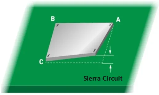
Figure. 6
5. Before plating, thin plates must be straightened:
A round stick should be attached to the entire flybar on the pinch rollers strung together in the automatic plating line on the flybar clamped on the 0.4 ~ 0.6 mm ultra-thin multilayer plate for surface plating and graphic plating. This will straighten the rollers on the entire board and prevent deformation of the board after plating.
Without this precaution, the plate will get distorted after a 20–30 micron layer of copper is plated, and this can be challenging to fix.
6.Hot air leveling following cooling of the board:
After removing the marble or steel plate, the printed board should be placed on a flat surface to cool naturally before being delivered to a post-processing machine for cleaning. The solder tank levels the hot air at a temperature of roughly 250 degrees Celsius. This helps to keep the board from warping.
A few seconds after removal, some factories level the plate hot air into the cold water to increase the brightness of the lead tin surface. This hot and cold shock is likely to cause blistering, delamination, or warping for particular types of boards.
For cooling, the apparatus can also be placed on the air-float bed.
7. Processing of warped boards:
In well-run factories, printed boards will undergo a 100% flatness check during the final inspection. Unqualified boards will be selected, baked at 150 degrees Celsius for three to six hours under high pressure, and then allowed to cool naturally.
After releasing the pressure to remove the board, check for flatness. Some boards can be saved by doing this, but others require two or three times the baking pressure to level. A portion of the board baking pressure is worthless and can be discarded if the aforementioned process steps for preventing warpage are not followed.
What is the PCB warpage standard?
Industry insiders refer to this phenomena as PCB warpage. The PCB warpage standard is the amount of circuit board bending that occurs when the original flat circuit board is put on the desktop at either end or in the center of the slightly upward warping.
The formula for circuit board warpage, which is determined by placing the board on the desktop with its four corners on the floor and measuring the height of the center arch, is as follows: warpage = arching height / PCB long side length * 100%.
Industry standards for board warpage: The production of circuit boards permits a maximum warpage and distortion of 0.75 to 1.5 percent between the process capacities of each factory. This is in accordance with the U.S. IPC-6012 (1996 version) "rigid printed circuit board identification and performance specifications." There are also some differences for the PCB warpage control requirements, such as for 1.6 board thickness conventional double-sided Most circuit board manufacturers regulate PCB warpage for conventional double-sided multi-layer circuit boards with a board thickness of 1.6 between 0.70 and 0.75 percent. Many SMT and BGA boards have requirements of 0.5%, while some circuit board factories have process capabilities that allow PCB warpage to be stronger, up to 0.3%.
How to prevent warpage of the circuit board during manufacture
The symmetry of the semi-cured arrangement between the layers, the proportion of the six-layer circuit board, and the thickness and quantity of semi-cured sheets between layers 1-2 and 5-6 should all be the same; ② PCB core boards with several layers, PCB core boards, PCB core boards, PCB core boards, and so on.
Products from the same provider should be utilized with a multi-layer PCB core board with a curing sheet; ③ outer layer It is important that the board's A and B sides match those of the outer layer.③ When the A side of the big copper surface is close to the B side of only a few lines, the etching will be very easy to see once warpage occurs. Therefore, the outer A side and the B side of the line graphic region should be as close as feasible.
Ways to stop the circuit board from warping
1. Engineering design: prepregs between layers should be arranged in a coordinated manner; multilayer boards' prepregs and core board should utilize products from the same source; the graphics area of the outer C/S surface should be as close as feasible, and independent grids can be employed;
2. Before unloading, bake the board at 150 degrees for 6 to 10 hours to remove moisture, cure the resin entirely, and alleviate stress from the board. Bake the board before cutting, whether it's the inner layer or both sides!
3. Take note of the board curing sheets' warp and weft directions before laminating multilayer boards, as the shrinkage ratios in these directions differ.
4. Stress is eliminated by lamination thickness. Trim the burrs after pressing the plate in a cold press;
5. Bake the plate for four hours at 150 degrees before drilling;
6. Special clamps are used during electroplating to prevent the plate from bending and folding; chemical cleaning is advised and mechanical brushing is not advised for thin plates.
7. Before cleaning, allow the tin to naturally drop to room temperature on a flat marble or steel plate or allow it to cool on an air flotation bed.


